
Intel walked into Hot Chips 2026 today with two chips and a single argument: the next wave of agentic AI infrastructure does not have to be built around NVIDIA. The two products carrying that argument are Diamond Rapids, its next-generation Xeon processor, and Crescent Island, an inference-only datacenter GPU.
The timing matters. Across mid-2026, datacenter operators are making a specific procurement call: whether to commit further to NVIDIA’s integrated ecosystem for inference workloads, or evaluate alternatives that slot into the air-cooled server fleets they already own. Intel is pitching a two-part answer, and it comes with two different planning horizons. Diamond Rapids carries a 2027 timeline, while Crescent Island is targeted for a 2026 market introduction.
This piece lays out what both chips actually do, how Intel has designed them to work together, and the execution risks that sit between today’s disclosure and a production rack. The goal is a technically grounded read on both products and their combined market logic, not a rehash of the press deck.
Two chips, one thesis: how Intel is framing the agentic AI infrastructure problem
Before the specifications, understand the argument Intel is making, because everything else reads as evidence for it.
At Hot Chips 2026, Intel characterised agentic AI (software agents that reason, act, and coordinate across multiple steps) as a problem of balancing computational performance against cost efficiency across different deployment tiers. That framing is deliberate. If the workload spans orchestration, security, and high-volume token generation, a single accelerator is the wrong shape for the job. Two specialised layers are the answer Intel has chosen.
The division of labour is clean:
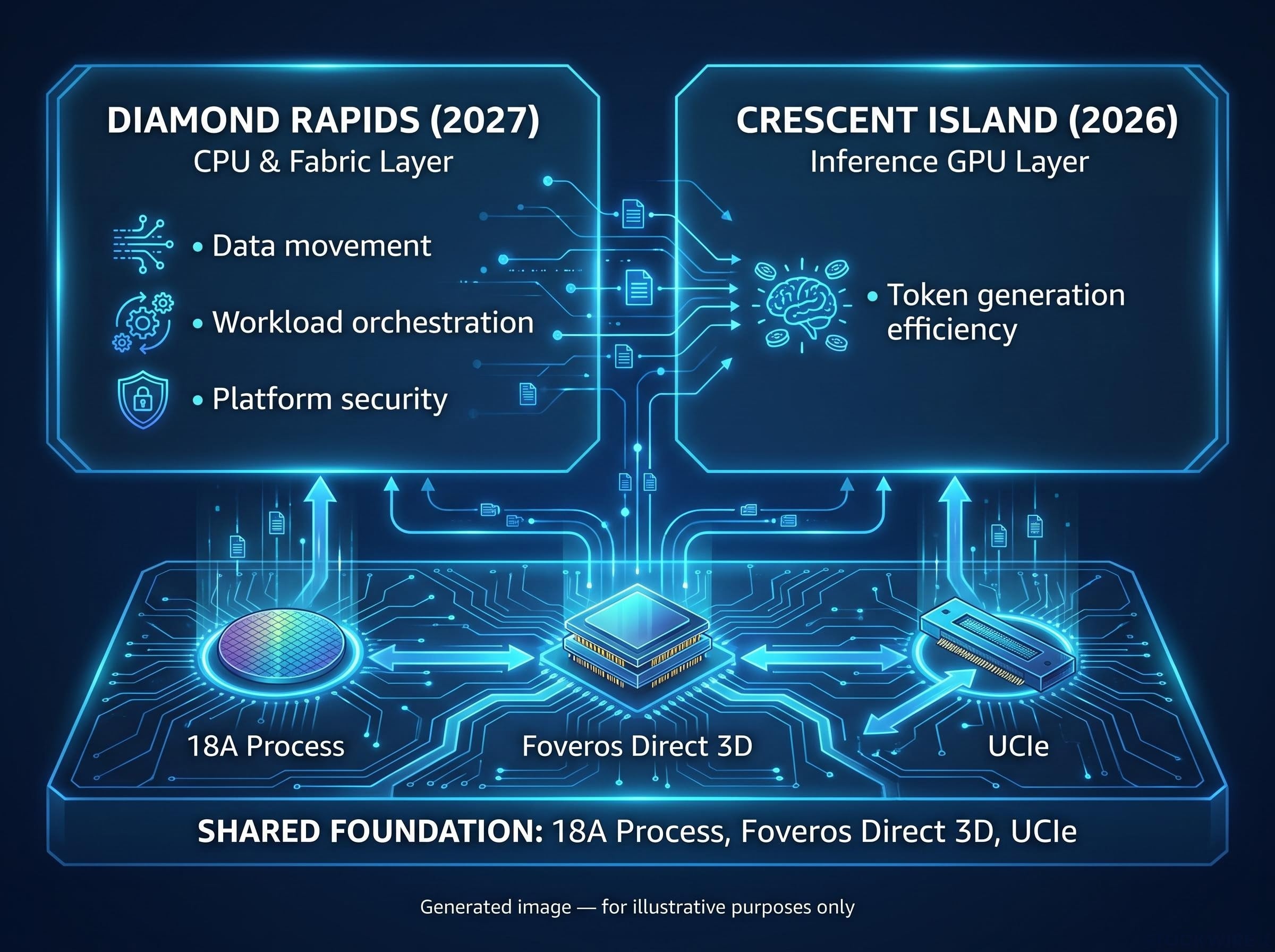
- Diamond Rapids (the CPU and fabric layer) handles data movement, workload orchestration, and platform security across accelerators.
- Crescent Island (the inference GPU layer) handles token generation efficiency, optimised for output per watt rather than peak throughput.
Both products sit on Intel’s 18A process family, use Foveros Direct 3D packaging, and adopt UCIe chiplet interconnect standards. That shared foundation is not incidental; it signals a unified manufacturing platform underneath a deliberately split product strategy.
The competitive argument here is worth stating plainly, because it is not the one most people expect. Intel is not claiming training-performance parity with NVIDIA. It is arguing infrastructure practicality: chips that deploy inside existing air-cooled servers, at a cost-per-inference profile pitched at enterprise workloads rather than hyperscaler training clusters.
Custom silicon competition from Alphabet, Amazon, and Microsoft, all of which are building inference-optimised accelerators specifically to reduce NVIDIA dependency, gives Intel’s enterprise positioning argument a structural tailwind: procurement teams already have reasons to evaluate alternatives before Intel ships a single Crescent Island card.
What that tells you is that Intel is betting the next procurement cycle gets decided on inference economics and deployment flexibility, not peak training FLOPS. Whether that bet pays off depends entirely on execution timing, and that timing is still unresolved.
When big ASX news breaks, our subscribers know first
What the specifications actually say about each chip’s design priorities
The specifications are where the strategy stops being rhetoric and starts being silicon. Read against the design intent, the numbers show what Intel prioritised and, just as tellingly, what it gave up.
Start with Diamond Rapids. It is a 16-chiplet design, 16 cores per chiplet, for up to 256 Panther Cove P-cores across four Intel 3-T base tiles. That is a lot of scalar compute, but the more revealing numbers are around data movement: 1.28 GB of last-level cache, up to 16 channels of DDR5 or MRDIMM delivering roughly 1.6 TB/s of aggregate bandwidth, and 128 PCIe Gen6 lanes plus 8 PCIe Gen4 lanes. According to SemiWiki’s 27 August 2026 analysis, the chip’s fan-out fabric is built around moving and protecting data as efficiently as executing instructions, which is the point. This is a CPU designed to orchestrate accelerators, not to be the accelerator.
| Parameter | Value | Design rationale |
|---|---|---|
| Cores | Up to 256 Panther Cove P-cores | Scalar throughput for stateful agentic services |
| Last-level cache | 1.28 GB | Keeps large working sets close to compute |
| Memory bandwidth | ~1.6 TB/s (16-channel MRDIMM) | Feeds data movement at scale |
| PCIe | 128 Gen6 (CXL 3.0/UPI 3) + 8 Gen4 | Fabric to orchestrate attached accelerators |
| Process / packaging | 18A-P; Foveros 3D Direct, UCIe-S | Advanced node plus modular multi-tile assembly |
Diamond Rapids also carries AMX (enhanced Advanced Matrix Extensions for AI math), AVX 10.2, and Intel TDX and SGX security features, reinforcing the orchestration-and-protection role.
Crescent Island tells a sharper story, largely through what is missing. It uses 32 Xe3P cores, 256 XMX engines, 256 vector engines, 32 MB of L2 cache, and supports data types from FP4 and MXFP4 through FP64. Intel deliberately stripped out 3D and ray-tracing hardware.
| Parameter | Value | Design rationale |
|---|---|---|
| Xe3P cores / XMX engines | 32 cores, 256 XMX engines | Die area concentrated on inference math |
| Memory | 160 GB reference, up to 480 GB LPDDR5X | Large-model capacity without HBM |
| TDP / interface | 350 W, PCIe Gen5 x16 | Fits standard air-cooled server slots |
| Data types | FP4/MXFP4 through FP64 | Versatility across low-precision inference |
| 3D / ray-tracing hardware | Removed | Power and area reallocated to tokens-per-watt |
That removal is the most telling signal in either chip. Intel has committed the die area and power budget entirely to tokens-per-watt, which means any enterprise weighing this card needs confidence their inference workload does not require the versatility a mixed-use GPU provides.
On the enhanced 18A-P node used for Diamond Rapids, HyperAI’s 24 August 2026 analysis cites a 9% performance uplift at peak frequency or an 18% power reduction versus standard 18A. These are vendor-stated figures. No independent benchmark confirms them as of today.
Which points to the broader caveat: no MLPerf, SPEC, or equivalent third-party scores exist for either product as of 1 September 2026. Every number above describes intent, not measured performance.
The LPDDR5X bet and the inference market Intel is targeting
The single most consequential decision in Crescent Island’s design is the memory. Intel chose LPDDR5X over the high-bandwidth memory (HBM) that sits on NVIDIA’s training-class accelerators, and that choice is the lens through which the whole inference strategy becomes legible.
The logic is a power argument. LPDDR5X lets Crescent Island reach up to 480 GB of capacity while holding a 350 W TDP, which keeps it inside standard air-cooled server envelopes. Slot it into a PCIe Gen5 x16 connector and it runs in the datacenter infrastructure operators already own, no liquid-cooling upgrade required. For enterprise buyers, that is a direct cost and logistics advantage.
The trade-off is equally direct. Here is how the two memory approaches stack up:
HBM market dynamics explain why Intel’s LPDDR5X choice is a deliberate departure rather than a cost compromise: the HBM market is projected to reach $100 billion by 2028 at mid-80% gross margins, a pricing environment that makes LPDDR5X-based designs structurally cheaper to produce and more accessible for enterprise buyers outside hyperscaler budgets.
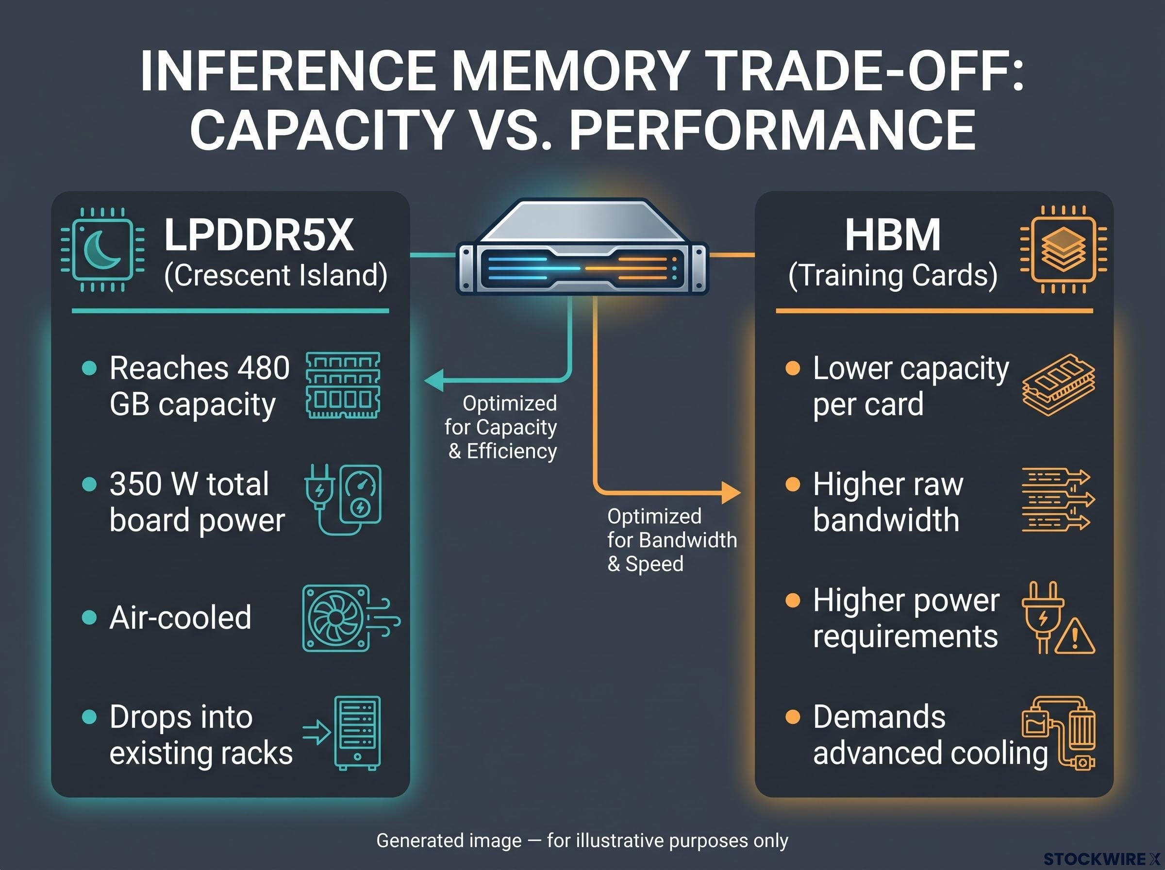
- Capacity ceiling: LPDDR5X reaches 480 GB at manageable power; HBM configurations typically top out lower per card.
- Bandwidth profile: HBM’s raw bandwidth is materially higher, which favours the most demanding, throughput-hungry inference.
- Power envelope: LPDDR5X keeps total board power at 350 W, air-cooled; HBM designs push power and cooling requirements far higher.
- Infrastructure requirements: LPDDR5X drops into existing racks; HBM training cards often demand denser power and advanced cooling.
The honest read is that this leaves Crescent Island likely to trail NVIDIA’s H-series and Blackwell accelerators on raw tokens-per-second for the heaviest workloads, even if it competes on tokens-per-watt at lower throughput demands. No quantified cost-per-inference comparison exists in current sources, so that competitive framing stays qualitative for now.
The market segment Intel is actually chasing follows from this. It is targeting enterprise inference where model size and infrastructure simplicity matter more than peak throughput, as distinct from the hyperscaler training clusters where NVIDIA’s ecosystem is entrenched.
For an operator evaluating the card, the practical question is whether your workload is memory-capacity-bound, where 480 GB of LPDDR5X is a genuine advantage, or bandwidth-bound and latency-sensitive at scale, where the HBM gap will surface in production benchmarks that do not yet exist publicly.
Execution timeline and the risks Intel still has to clear
Product characterisation is one thing. Delivery is another, and here the facts speak for themselves.
Diamond Rapids has slipped to 2027. The Register’s 25 August 2026 coverage framed this bluntly as another schedule slip in Intel’s Xeon roadmap. No specific quarter has been confirmed.
Intel’s foundry credibility received its most significant external validation in June 2026 when the Apple chip manufacturing agreement confirmed that at least one tier-one customer viewed 18A as production-viable, a signal that directly bears on whether Diamond Rapids and Crescent Island can attract the enterprise partnerships that would validate today’s disclosure.
“Delayed until 2027.” That was The Register’s characterisation of the Diamond Rapids timeline in its coverage dated 25 August 2026.
The risks fall into three distinct categories, in priority order:
- Schedule risk. Diamond Rapids is now a 2027 product with no confirmed quarter, extending a roadmap pattern that operators planning around it will need to account for.
- Manufacturing and yield risk. The 16-chiplet Foveros 3D Direct design on the 18A-P node requires advanced packaging and a new process to ramp together. No independent yield data is publicly available.
- Deployment evidence risk. As of late August 2026, no named enterprise or hyperscaler deployments of either chip have been cited, and no third-party benchmarks exist.
Crescent Island’s 2026 target also lacks a confirmed quarter as of today’s disclosure, beyond the original 2025 framing from Tom’s Hardware.
What this means for planning is straightforward. Any infrastructure roadmap built around either chip in 2026 carries roadmap risk that needs to be priced in, particularly for Diamond Rapids, where the 18A-P process ramp and packaging complexity have not been independently validated. For investors and procurement teams alike, this is where announced capability meets delivery track record, and Intel’s ability to execute on both 18A-P yield and Foveros packaging at this complexity is the variable that decides whether today’s disclosure becomes market share by 2027.
What the 18A-P strategy means for Intel’s datacenter position through 2027
Step back, and a coherent picture emerges. All three architectures Intel showed at Hot Chips 2026 share the 18A process family, Foveros Direct 3D packaging, and UCIe interconnects, which points to a unified manufacturing platform underneath the product line.
The combined Diamond Rapids and Crescent Island play is an attempt to compete with NVIDIA on a different axis: infrastructure practicality and inference economics rather than peak training throughput. The differentiation centres on tokens-per-watt for Crescent Island and data movement, security, and orchestration for Diamond Rapids, not training FLOPS parity.
The technical differentiation is genuine on paper. A 256-core CPU with 1.6 TB/s memory bandwidth and 128 PCIe Gen6 lanes, paired with a 480 GB inference GPU at 350 W, is a specific and defensible architectural bet. What it is not, yet, is independently validated.
Three variables will tell you whether the bet holds:
- 18A-P yield and ramp progress, the gating factor for Diamond Rapids’ competitiveness.
- Crescent Island named deployment announcements, the first real evidence of market traction.
- Intel’s software ecosystem development around both products, and whether it narrows the gap with NVIDIA’s incumbent developer tooling.
Intel has made a specific, coherent bet on enterprise inference and agentic orchestration. Its outcome is gated on manufacturing execution and software development that will not be visible until the 2026-2027 timelines actually play out.
Intel’s broader platform strategy extends well beyond these two chips: its ZAM stacked DRAM consortium with SoftBank, the XBM patent targeting UCIe-based memory integration, and a $20 billion equity raise closed in August 2026 collectively signal that Diamond Rapids and Crescent Island are pieces of a larger memory-compute architecture rather than standalone product bets.
This article is for informational purposes only and should not be considered financial advice. Investors should conduct their own research and consult with financial professionals before making investment decisions. Past performance does not guarantee future results, and forward-looking product timelines are subject to change based on manufacturing execution and market conditions.