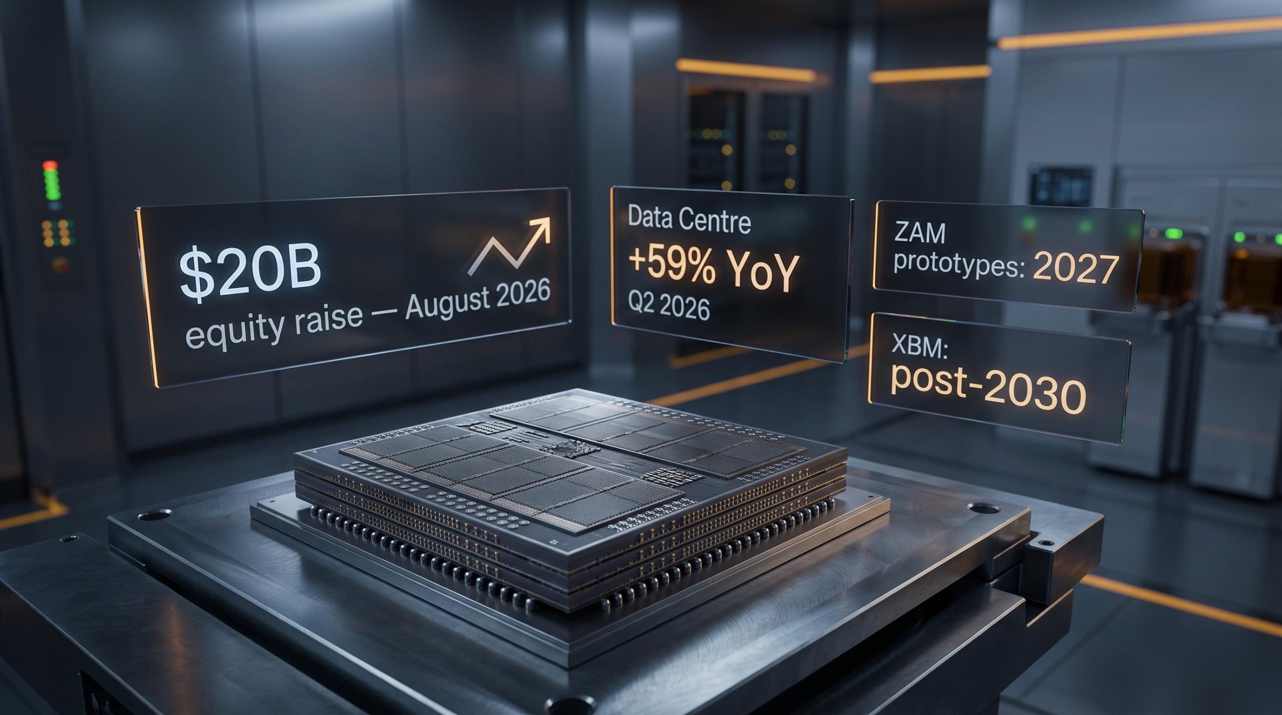
Intel has not sold a memory chip in four years. Yet in the space of six months, the company filed a landmark memory patent, signed a formal stacked DRAM partnership, hired the former chief executive of the world’s largest memory maker, and raised $20 billion in its first equity offering since 1971. That is not a rumour cycle. That is a pattern.
On 13 August 2026, CEO Lip-Bu Tan spoke on the TechSurge: Deep Tech VC Podcast and made clear that next-generation memory architecture sits at the top of his personal agenda, language that carried genuine weight given the infrastructure already assembled around it. The question investors now face is not whether Intel is moving toward memory, but how to read a situation where the technical commitments are concrete and the corporate governance is deliberately opaque.
Here is what the confirmed evidence actually supports, where the ambiguity sits, and which signals would turn this strategic trajectory into a committed business line, so you can assess what Intel’s memory push means for its competitive positioning without confusing direction with destination.
Intel already has two concrete memory bets, not just a CEO hint
Tan’s language on the podcast was carefully hedged: “We are not ready to unfold it.” But the programmes he was referring to are not hedged at all. Two distinct memory architectures are already in development, each backed by formal partnerships, filed intellectual property, and multi-region industrial support. The ambiguity lives at the corporate disclosure level, not the engineering level.
Z-Angle Memory: a multi-region industrial bet
In February 2026, Intel announced a formal collaboration with SoftBank’s SAIMEMORY subsidiary to develop Z-Angle Memory (ZAM), a stacked DRAM technology targeting AI and high-performance computing workloads. SAIMEMORY leads development and commercialisation; Intel is the architecture and standards partner. The consortium includes Taiwan’s PSMC, Japan’s Shinko Electric, and research entity RIKEN, making ZAM a multi-region industrial initiative rather than a single-company research project.
Prototypes are targeted for 2027, with volume commercialisation around 2029-2030.
Cross-Batch Memory: the patent that removes the interposer
Intel’s Cross-Batch Memory (XBM) patent was filed on 26 December 2024 and, according to TrendForce, appeared in public records on 2 July 2026. The architecture does away with the conventional silicon interposer found in current High Bandwidth Memory (HBM), substituting UCIe-based serial links and BEOL (back-end-of-line) transistors in its place. UCIe is a standard for connecting chiplets, the modular building blocks of modern processors. BEOL transistors are fabricated in the final manufacturing layers, allowing tighter integration without redesigning the base chip.
XBM is designed to match the performance regime expected of future HBM4, with a commercialisation timeline that extends beyond 2030.
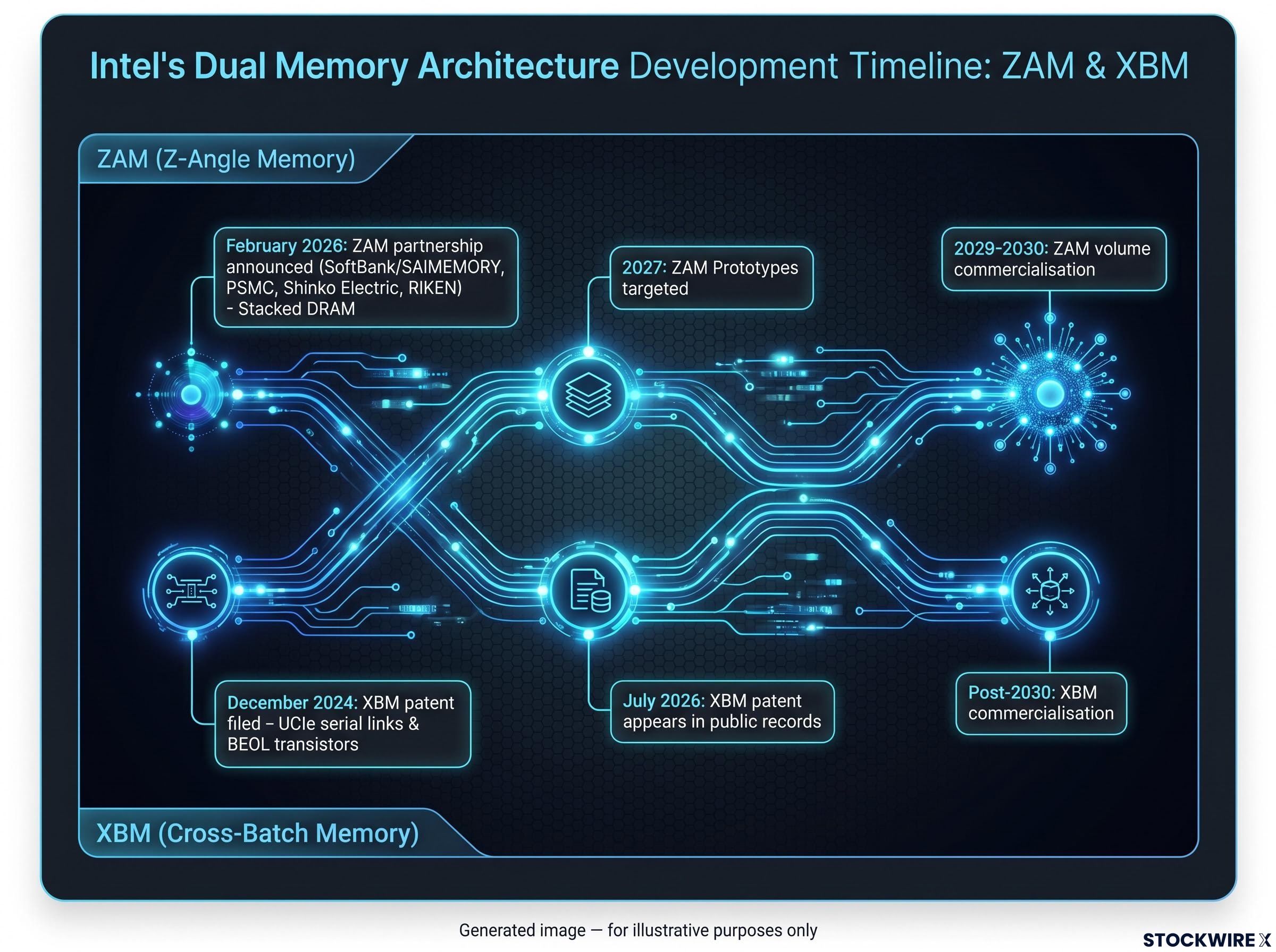
Both programmes share a critical characteristic: they target post-HBM, AI-centric memory and sit on a 2029-2030 horizon. This is a long-dated strategic bet, not a near-term revenue play. But the existence of formal partnerships, filed patents, and a multi-region consortium means you can treat ZAM and XBM as engineering-level commitments, not speculation, even though no standalone memory business unit has been announced.
| Programme | Partner(s) | Architecture Approach | Timeline | Intel’s Role |
|---|---|---|---|---|
| ZAM (Z-Angle Memory) | SoftBank/SAIMEMORY, PSMC, Shinko Electric, RIKEN | Stacked DRAM for AI/HPC capacity and power efficiency | Prototypes 2027; commercialisation 2029-2030 | Technology and standards partner |
| XBM (Cross-Batch Memory) | Intel (internal patent) | UCIe serial links and BEOL transistors replacing silicon interposer | Post-2030 commercialisation | Patent holder and architect |
When big ASX news breaks, our subscribers know first
Why Intel is entering memory as a system architect, not a chip vendor
The instinct when hearing “Intel memory chips” is to benchmark against SK Hynix, Samsung, and Micron, the companies that dominate memory through manufacturing scale and cost-per-bit efficiency. That benchmark leads to the wrong analytical conclusion.
Intel’s ZAM and XBM programmes are not bids to produce commodity DRAM more cheaply. They are premised on tight integration with Intel’s foundry, advanced packaging, and UCIe chiplet ecosystem. The competitive thesis rests on whether AI chip buyers value tightly coupled compute-near-memory solutions enough to design around Intel’s architecture. That is a different investment question from whether Intel can manufacture DRAM at competitive margins.
Intel’s data centre chip division expanded 59% year-over-year in Q2 2026, confirming that AI workloads are already the company’s growth engine. Memory bandwidth is the constraint those workloads keep hitting. XBM commentary consistently emphasises integration with UCIe chiplet ecosystems and AI accelerators, positioning Intel’s potential moat at the system architecture layer rather than the fabrication layer.
The HBM demand trajectory Intel is positioning around is more pronounced than most forecasts capture: Citi projects a 434% surge in system-level HBM capacity requirements as AI deployments scale from 72 to 576 GPUs per system, while per-chip HBM content has already grown 3.6x from the H100 to the Rubin generation, making both vectors additive tailwinds rather than substitutes.
UCIe Consortium membership includes Intel, AMD, Arm, TSMC, Samsung, and NVIDIA as promoter members, confirming that the chiplet interconnect standard underpinning XBM has broad industry backing rather than being a proprietary Intel specification unlikely to achieve ecosystem adoption.
Intel has tried adjacent memory bets before, and each one failed:
- Hybrid Memory Cube (HMC): Abandoned; lacked ecosystem adoption.
- MCDRAM (Multi-Channel DRAM): Discontinued with Knights Landing; niche performance product with limited market.
- Optane: Discontinued approximately four years ago after persistent commercial underperformance despite genuine technical differentiation.
All three competed on architecture without the financial runway or ecosystem depth to sustain the bet. The current push arrives with materially different resources.
The memory market structure Intel is entering has changed in ways that make the current push structurally different from the Optane era: AI data centre operators now account for an estimated 70% of total memory shipment volumes, SK Hynix has shifted to foundry-style multi-year supply agreements extending through 2028-2030, and hyperscaler capex is projected to reach $725 billion in 2026 alone.
“We are not ready to unfold it.” — Lip-Bu Tan, CEO, Intel, TechSurge podcast, 13 August 2026
If Intel’s moat is integration rather than scale, the programmes succeed or fail based on whether AI system builders adopt UCIe-based chiplet designs at a rate that justifies memory-compute coupling. SK Hynix’s DRAM market share matters less to that thesis than the adoption curve of UCIe itself.
What the $20 billion equity raise signals, and what it does not
Intel closed a $20 billion common stock offering on 10 August 2026, upsized from an initial $15 billion target. Key details:
- Shares priced at $95 each
- Approximately 210.5 million shares issued
- Tan committed $12 million drawn from his own resources and those of his family, buying in at the same offering price as other investors
- Closing date: 10 August 2026
This was Intel’s first equity issuance since its 1971 IPO, a gap of more than five decades.
Tan’s personal investment at the offering price is a commitment signal. But the official use-of-proceeds language is deliberately broad: “general corporate purposes,” including capital expenditures and working capital. There is no explicit earmark for a memory business.
That ambiguity matters for modelling. The raise removes capital scarcity as a constraint on scaling ZAM and XBM, both of which depend on capital-intensive advanced packaging and interconnect technologies. But the absence of a formal memory-specific allocation means you cannot yet model the initiative as a discrete capex line. You can model it as a funded option, nothing more.
Investors wanting to model how Intel’s $20 billion raise interacts with the broader capex cycle will find our deep-dive into semiconductor equipment spending useful, covering Intel’s 40% year-over-year tool purchase growth and the coordinated domestic advanced packaging build-out that gives ZAM and XBM their manufacturing infrastructure context.
The honest read is that the $20 billion is both a dedicated war chest and a general balance sheet reinforcement, and the distinction shapes how much optionality you assign to the memory thesis versus Intel’s broader foundry ambitions.
This article is for informational purposes only and should not be considered financial advice. Investors should conduct their own research and consult with financial professionals before making investment decisions.
The Seok-Hee Lee appointment and the governance question it opens
Lee’s dual exposure: Intel Foundry and the Ohio facility talks
On 18 June 2026, Intel brought in Seok-Hee Lee, who had previously served as chief executive of SK Hynix, to fill the role of executive vice president of Intel Foundry. The hire signals genuine domain expertise: Lee ran the world’s largest HBM producer during the period when AI-driven memory demand reshaped the industry.
The tension is specific. According to separate reports, SK Hynix is in active negotiations that could result in the purchase of Intel’s Ohio chip facility for domestic US memory production. Lee now sits at the intersection of a former employer and a current employer with active commercial negotiations. There is limited public disclosure about what recusal protocols govern his involvement in those discussions.
Tan’s Walden International and the conflict-of-interest perimeter
Tan continues to hold the positions of founder and chair at Walden International, a venture capital firm he established that carries documented exposure to memory-ecosystem companies, including suppliers to Chinese NAND and DRAM players such as YMTC. Public reporting indicates this dual role has already drawn regulatory and political scrutiny.
The same appointment that signals domain expertise creates an unresolved governance risk. Unresolved questions include:
- The boundary between Intel’s institutional memory initiative and any Walden-linked investment thesis
- Board-level recusal protocols for memory-related decisions involving Tan’s personal portfolio
- How Lee’s prior SK Hynix relationships are managed relative to Intel’s foundry negotiations
The absence of detailed public disclosure on these points is not a minor reporting gap. It is the governance ambiguity that justifies caution about deal-flow conflicts between Intel’s memory initiative and Walden’s portfolio companies. Both Tan’s and Lee’s dual relationships will influence deal terms, IP access, and partner selection in ways that may not be visible in public filings.
Intel’s memory architecture, explained: why post-HBM matters for AI
Why the silicon interposer is HBM’s ceiling
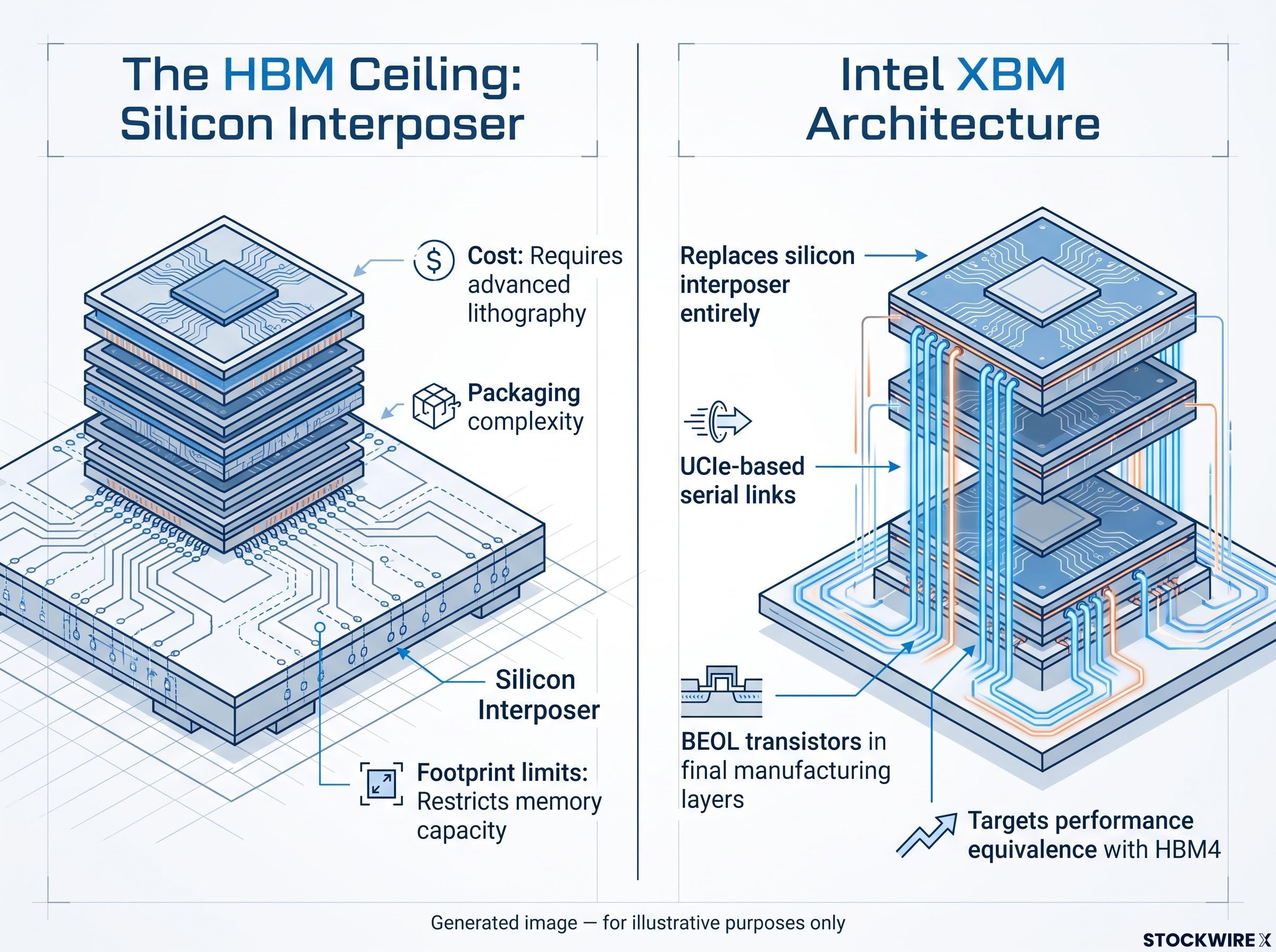
High Bandwidth Memory (HBM) is the current standard for AI accelerator memory. It works by stacking DRAM chips vertically and connecting them to a processor through a silicon interposer, a thin slice of silicon that acts as a high-speed wiring layer between the memory stack and the processor chip.
The interposer is also HBM’s constraint. Three factors create the ceiling:
- Cost: Silicon interposers require advanced lithography, making them expensive to produce at scale.
- Packaging complexity: Fitting interposer-based HBM stacks alongside large AI processors demands increasingly sophisticated packaging, limiting how many memory stacks can be placed near the compute.
- Footprint limits: The physical area consumed by the interposer restricts memory capacity per package, which matters as AI models grow larger and more memory-hungry.
How ZAM and XBM are designed to clear that ceiling
XBM’s architecture replaces the silicon interposer entirely with UCIe-based serial links, eliminating the cost and footprint constraints at the connection layer. BEOL transistors allow memory logic to be fabricated in the chip’s final manufacturing layers, enabling tighter integration with the compute die without a separate interposer substrate. The design targets performance equivalence with future HBM4.
ZAM attacks the problem from the capacity side. Its stacked DRAM model is designed to improve capacity and power efficiency relative to HBM for AI and HPC workloads, though specific capacity multiples cited in some coverage have not been independently verified.
Both programmes share a post-2030 volume commercialisation horizon. If you understand why the interposer is the bottleneck, Intel’s integration-first approach looks differentiated rather than derivative, which is the key to assessing whether the competitive thesis is credible on its own terms rather than benchmarking it against SK Hynix’s DRAM margins.
Five signals that would turn this trajectory into a confirmed business line
The gap between “strategic trajectory” and “committed business plan” is real. These are the five signals that would close it:
- A formal roadmap update explicitly integrating XBM and ZAM into Intel’s product and capex plans, with timelines and financial targets. Without this, the programmes remain engineering initiatives rather than business commitments.
- A detailed $20 billion allocation breakdown showing how capital distributes across foundry, packaging, and memory-adjacent initiatives. This would let you model memory as a discrete investment rather than an embedded option.
- New joint ventures, hires, or partnerships that deepen Intel’s role from technology partner toward direct manufacturing or exclusive supply. Movement here would signal a shift from architecture licensing to vertical integration.
- Board-level governance disclosure clarifying conflict-management protocols between Intel, Walden International, and Tan’s personal investments. This is a near-term watchpoint, not a long-dated one.
- Resolution of the Lee/SK Hynix conflict question, specifically whether and how Intel manages Lee’s dual exposure to Intel Foundry negotiations and his former employer’s potential Ohio facility acquisition.
ZAM prototypes are targeted for 2027, the nearest concrete technical milestone on this timeline.
The 2029-2030 commercialisation horizon means you have time to monitor these signals without a forced decision today. But the governance questions, Tan/Walden and Lee/SK Hynix, are the near-term items that could accelerate or complicate the thesis materially. Tracking both the technical milestones and the governance signals gives you a more complete picture than following patent filings alone.
These statements are speculative and subject to change based on market developments and company performance.
What the evidence settles, and what remains an investor’s call
For Q2 2026, Intel recorded revenue of $16.1 billion, a 25% increase year-over-year, while its share price has climbed roughly 180% year-to-date as of August 2026. The $20 billion equity raise closed on 10 August 2026. The financial recovery is real, and it removes the capital constraint that undermined every prior Intel memory venture.
Two concrete memory programmes are in development with engineering-level commitments. A strategic hire with direct domain expertise is in place. The CEO has publicly identified memory as a personal priority.
Intel’s memory push fits within a broader vertical silicon integration thesis that the company has been assembling across multiple sectors: its Computex 2026 partnerships with Foxconn, Siemens, and Hitachi all centre on purpose-built processors co-designed for specific industrial environments, a pattern that treats memory-compute coupling as one layer in a larger embedded-systems strategy rather than a standalone product bet.
What remains unresolved is equally specific: no standalone Intel memory business unit, P&L, or disclosure cadence exists as of publication. The governance boundary between Intel’s institutional initiative and Tan’s personal venture capital interests has not been drawn in public filings. No formal capex earmark has been disclosed.
| Confirmed Signals | Unresolved Items |
|---|---|
| ZAM partnership (February 2026) | Board-level governance/recusal protocols |
| XBM patent (filed December 2024, published July 2026) | Formal memory P&L or business unit |
| Seok-Hee Lee appointment (June 2026) | Dedicated capex earmark from $20B raise |
| $20 billion equity raise (August 2026) | Business unit structure and disclosure cadence |
| CEO public priority statement (August 2026) | Walden/Intel conflict perimeter definition |
The memory thesis is real enough to monitor closely and uncertain enough that treating it as settled strategy would be a mistake. A calibrated view, one that neither dismisses the signals nor front-runs the announcement, is what gives you an edge in positioning around a thesis the market is still pricing ambiguously.
—