Memory chips with mid-80% gross margins and persistent supply shortages are not behaving like commodities. They are behaving like strategic infrastructure, and the economics of High Bandwidth Memory (HBM) confirm that the semiconductor industry has quietly reclassified an entire product category.
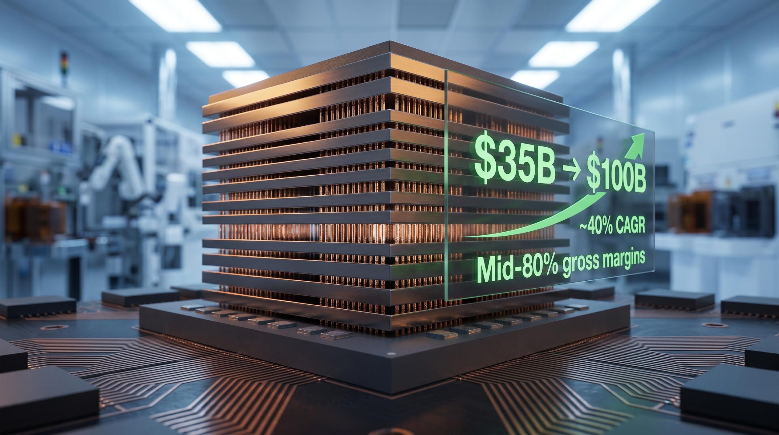
That reclassification is accelerating. According to Micron, the HBM market is projected to expand from around $35 billion in 2025 to approximately $100 billion by 2028, a milestone the company has reportedly brought forward by roughly two years as AI infrastructure build-out accelerates ahead of earlier expectations. Intel’s entry into this space, through two architecturally distinct memory bets called XBM and ZAM, signals that even a company fighting for its foundry survival sees memory as territory worth contesting.
Here is the framework for understanding where HBM exposure actually sits today, what Intel’s patents and partnerships signal about the 2030 supply picture, and how to size and time positions across the two very different risk profiles available: near-term incumbent dominance and long-duration Intel optionality.
Why memory stopped being a commodity business
The mid-80% gross margins Micron reports in its memory segment did not arrive through pricing luck. They are a structural consequence of what it takes to manufacture HBM at scale.
Each generation of HBM stacks more layers of DRAM vertically, from 8 layers in current HBM3E configurations to 12-16 in HBM4, with 20-layer stacks on the development horizon. Every additional layer compounds yield risk. Align thousands of through-silicon vias (TSVs), tiny vertical electrical connections that link each layer, across a taller and taller stack, and the probability of a defective unit rises with each tier added. As analysts have noted, there is “no way to solve the supply problem before new fabs are completed.”
DRAM supply constraints are proving more stubborn than capital alone can resolve: SK Hynix projects tightness through 2030, HBM inventory industry-wide sits at roughly 3-4 weeks, and Google CEO Sundar Pichai has identified memory availability rather than capital budgets as the binding limit on AI infrastructure expansion.
The growth forecast tells you the same story from the demand side. HBM content per GPU accelerator is rising, meaning each chip shipped requires more HBM. That is what drives a roughly 40% compound annual growth rate through 2028, not simply more units leaving the factory.
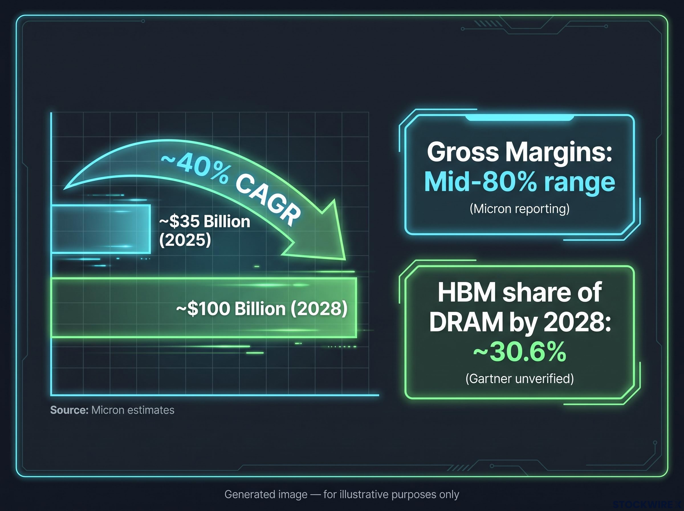
| Metric | Value | Source |
|---|---|---|
| HBM market size (2025) | ~$35 billion | Micron estimates |
| HBM market size (2028 forecast) | ~$100 billion | Micron estimates |
| Implied CAGR (2025-2028) | ~40% | Derived from Micron estimates |
| Memory segment gross margins | Mid-80% range | Micron reporting |
| HBM share of DRAM by 2028 | ~30.6%* | Gartner (*unverified estimate) |
Industry research suggests HBM bit demand for AI server chips could grow roughly 35x by 2028 (an unverified industry estimate), which would further reinforce the structural nature of this cycle. What the margin and supply data tell you together is that HBM incumbents hold a pricing position rooted in manufacturing difficulty, not a cyclical peak. That distinction matters for how durable this opportunity looks across a multi-year horizon.
Omdia DRAM market dynamics research projects HBM’s share of total DRAM revenue surpassing 30% by 2026, a trajectory consistent with the supply-side structural argument that pricing power in this segment reflects manufacturing scarcity rather than a cyclical peak.
When big ASX news breaks, our subscribers know first
How HBM actually works, and why the manufacturing is so hard
What makes HBM different from standard DRAM
Standard DRAM sits flat on a circuit board, communicating through traces etched across the surface. HBM does something fundamentally different. It stacks multiple DRAM dies vertically, one on top of another, connecting them through thousands of TSVs (through-silicon vias, essentially tiny copper pillars drilled through each layer of silicon). The entire stack is then mounted on a silicon interposer, a large piece of silicon that sits underneath and connects the memory stack to the GPU or AI accelerator die beside it.
Bandwidth scales with layer count: more layers means more parallel data paths. But yield risk scales just as quickly. Every additional layer multiplies the points at which a single misaligned via or bonding defect can render the entire stack unusable.
Why packaging expertise is the real bottleneck
The barrier to entry is not raw DRAM fabrication skill. It is the advanced packaging expertise required to stack, align, bond, and thermally manage these increasingly tall structures. Key manufacturing complexity factors include:
- Layer stacking precision across 8-16 (and eventually 20+) dies
- TSV alignment tolerances measured in micrometres
- Advanced packaging and bonding processes
- Thermal management as stack height increases
- Yield sensitivity that compounds with each additional layer
As Omdia and industry analysts have noted, supply constraints cannot be resolved before new fab and packaging capacity comes online. Lee Jong-hwan, professor of system semiconductor engineering at Sangmyung University, observed in August 2026 that “transitioning new memory concepts through verification, commercialisation, and volume production is exceptionally challenging.” That observation applies directly to what SK hynix, Samsung, and Micron have spent years learning, and to the gap any new entrant must close. Their multi-generation head start in advanced packaging amounts to a structural barrier, not a temporary lead that capital alone can overcome.
Intel’s XBM bet: a different architecture, not just a different brand
Cross-Batch Memory (XBM) is Intel’s attempt to solve HBM’s cost problem by redesigning the architecture from the ground up rather than replicating what incumbents already do. According to TrendForce, the relevant patent was submitted on 26 December 2024 and entered the public record on 2 July 2026. Internal Asia-region reports suggest a commercialisation target of approximately 2030. No official timeline has been disclosed by Intel.
The architectural departure is deliberate. Instead of HBM’s approximately 3,000-trace parallel bus routed through an expensive silicon interposer, XBM serialises data over UCIe (Universal Chiplet Interconnect Express) links. UCIe is an open standard that allows chiplets, small modular chips, to communicate on a shared package. Patent analyses suggest XBM targets link speeds of approximately 32 GT/s per lane (unverified). Key architectural elements include:
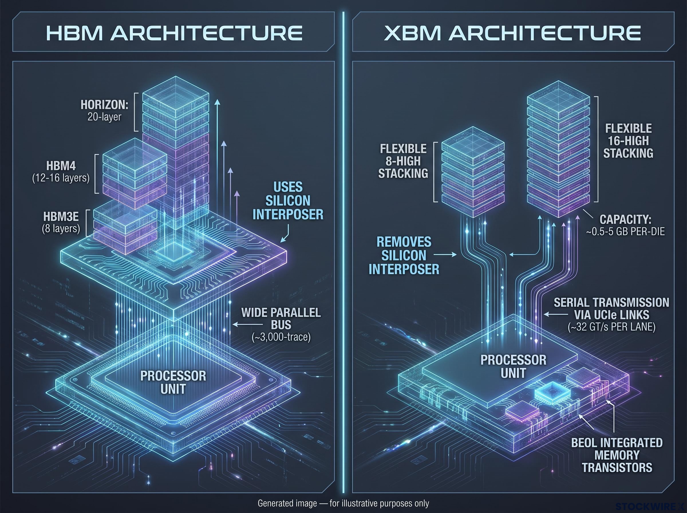
- Memory transistors integrated into the chip’s upper metal layers using a back-end-of-line (BEOL) process, eliminating the need for a discrete memory die
- Serial data transmission via UCIe links in place of a conventional wide parallel bus
- Removal of the silicon interposer from the package design entirely
- Flexible stacking configurations (8-high or 16-high, with per-die capacity of approximately 0.5-5 GB, both unverified)
Lee Jong-hwan, professor of system semiconductor engineering at Sangmyung University, noted that “transitioning new memory concepts through verification, commercialisation, and volume production is exceptionally challenging,” regardless of how promising the underlying concept may be.
What XBM’s architecture tells you is that Intel is not trying to beat SK hynix at its own game. It is betting that the next generation of AI accelerators will value chiplet integration and interposer elimination enough to create an opening for a structurally different approach, one that leverages Intel’s foundry and chiplet strengths rather than competing on packaging expertise it does not yet possess.
Intel’s vertical integration strategy across industrial automation, life sciences, and digital infrastructure provides the broader context for why XBM and ZAM are coherent bets within the same corporate logic: a company redesigning itself around embedded, purpose-built silicon has strong structural incentives to own the memory architecture that sits inside those systems.
ZAM and the SoftBank angle: lower power, different ambition
Z-Angle Memory (ZAM) takes a more commercially legible path than XBM. A joint effort by Intel and SAIMEMORY, the SoftBank-owned memory venture, ZAM is a nine-layer stacked DRAM built around efficiency and density rather than raw peak bandwidth. In hyperscaler data centres, where energy cost is increasingly the binding constraint on AI deployment, that trade-off targets a genuine procurement priority.
The partnership structure splits responsibilities: Intel contributes technology and standards, while SAIMEMORY leads commercialisation and deployment. The collaboration was announced in February 2026, with joint development starting approximately Q1 2026, prototypes targeted for approximately 2027, and commercial deployment aimed at approximately 2029-2030.
| Attribute | HBM (Current) | ZAM (Claimed) | Verification Status |
|---|---|---|---|
| Capacity | Baseline | 2-3x HBM | Intel-SAIMEMORY disclosure |
| Bandwidth | Baseline | At least competitive | Intel-SAIMEMORY disclosure |
| Power consumption | Baseline | Up to ~50% lower | Intel-SAIMEMORY disclosure |
| Production cost | Baseline | Up to ~60% lower | Nikkei-cited reports (unverified) |
The claimed 60% production cost reduction, cited in Nikkei-sourced reports, has not been independently verified. If accurate, it would represent a significant disruption to HBM economics, but the figure should be treated with caution until prototype data is available.
ZAM’s power and cost claims, if even partially validated in prototypes by 2027, would represent a genuine threat to HBM’s dominance in hyperscaler deployments specifically, where energy efficiency is already reshaping procurement priorities. For SoftBank investors, ZAM’s success would also reinforce the narrative that SoftBank is building positions across the full AI infrastructure stack.
The incumbent moat and where Intel actually stands
Before weighing Intel’s memory bets, it is worth feeling the scale of the lead they are trying to close. SK hynix, Samsung Electronics, and Micron Technology are currently shipping and ramping HBM3E and HBM4-class products. They are not standing still while Intel files patents.
What incumbents are accumulating while Intel is still developing
During the roughly 40% CAGR growth period through 2028, incumbents are compounding three advantages simultaneously. Yield learning improves with every wafer processed. Customer relationships deepen as GPU vendors like Nvidia and AMD qualify specific HBM suppliers into their accelerator designs. And the infrastructure investment in new packaging capacity raises the benchmark any challenger must clear.
That benchmark keeps moving. The sequential execution hurdles Intel must clear before either XBM or ZAM reaches commercial scale are substantial:
- Validate a novel memory architecture (BEOL DRAM for XBM, nine-layer stacking for ZAM)
- Achieve reliable high-speed interconnect operation (UCIe for XBM, proprietary interfaces for ZAM)
- Reach HBM-competitive yields at volume
- Win design slots in fiercely competitive AI accelerator platforms against entrenched suppliers
Each of these steps takes years, and the incumbents’ position strengthens throughout. That gap is not a reason to dismiss Intel’s memory bets entirely, but it determines appropriate position sizing for any investor weighting XBM or ZAM in their Intel thesis.
Sizing the opportunity correctly: where to place AI-memory exposure now
The incumbent case, SK hynix, Samsung, and Micron, remains the most defensible near-term vehicle for the $100 billion HBM opportunity. These companies offer direct linkage to current AI memory economics, though their valuations already reflect significant upside.
HBM pricing mechanics extend well beyond the memory supplier tier: Bernstein projects a 2-2.5x contract price increase for 2027 that amplifies approximately fourfold at the hyperscaler purchase level once GPU vendors apply margin preservation, creating a repricing cascade that touches every layer of the AI supply chain.
Intel’s XBM and ZAM are long-duration optionality, not a current earnings driver. They should be anchored to Intel’s foundry and chiplet strategy rather than evaluated in isolation. Three dimensions of the Intel case matter:
- The foundry turnaround is the primary thesis anchor
- XBM and ZAM represent late-decade optionality
- Any credible prototype or design-win milestone would act as a sentiment catalyst
The right question is not “should I own Intel for the memory story” but “what specific evidence would make the memory story a material part of the Intel thesis.” The answer is milestone-driven, not calendar-driven. Four signals to monitor:
- HBM pricing, content per GPU, and capacity announcements from SK hynix, Samsung, and Micron, to gauge how quickly the $100 billion TAM is materialising
- Intel Foundry strategy updates that explicitly reference XBM, ZAM, or UCIe-centric memory solutions
- Technical disclosures or prototype demonstrations of XBM and ZAM, with bandwidth, power, and cost data versus HBM3E or HBM4
- Announced design wins or pilot deployments of ZAM or XBM in AI accelerators or hyperscaler data centres
The 2027 ZAM prototype target is the first concrete milestone that would begin converting ZAM from optionality to evidence.
For investors building the Intel foundry thesis before adding memory optionality, our deep-dive into Intel’s Q2 2026 earnings separates the $11 billion GAAP loss from the underlying operational picture, including the DCAI segment’s 59% revenue growth and the $2 billion foundry operating loss that defines the turnaround’s current cost.
What the HBM race tells you about where AI infrastructure value is settling
The HBM market’s economics, 40% CAGR, mid-80% gross margins, persistent supply tightness, confirm that memory has completed its transition from commodity to strategic infrastructure. This is a durable shift, not a cycle.
Intel’s XBM and ZAM bets are themselves evidence of where AI infrastructure value is migrating, regardless of whether Intel ultimately captures any of it. A company restructuring its entire business around a foundry model does not file memory architecture patents and partner with SoftBank subsidiaries on speculative whims.
The more likely scenario through 2028-2030 is not a binary outcome where one winner takes everything. Incumbents will likely dominate while new entrants prove themselves in adjacent or complementary niches. A layered allocation approach, primary exposure through incumbents, long-dated optionality through Intel’s broader foundry thesis, is more coherent than an either-or call. As Lee Jong-hwan observed, even compelling memory architectures face exceptional commercialisation hurdles, and the market will not wait for them.
This article is for informational purposes only and should not be considered financial advice. Investors should conduct their own research and consult with financial professionals before making investment decisions. Forward-looking statements regarding market size forecasts, commercialisation timelines, and product specifications are subject to change based on market developments and company performance.