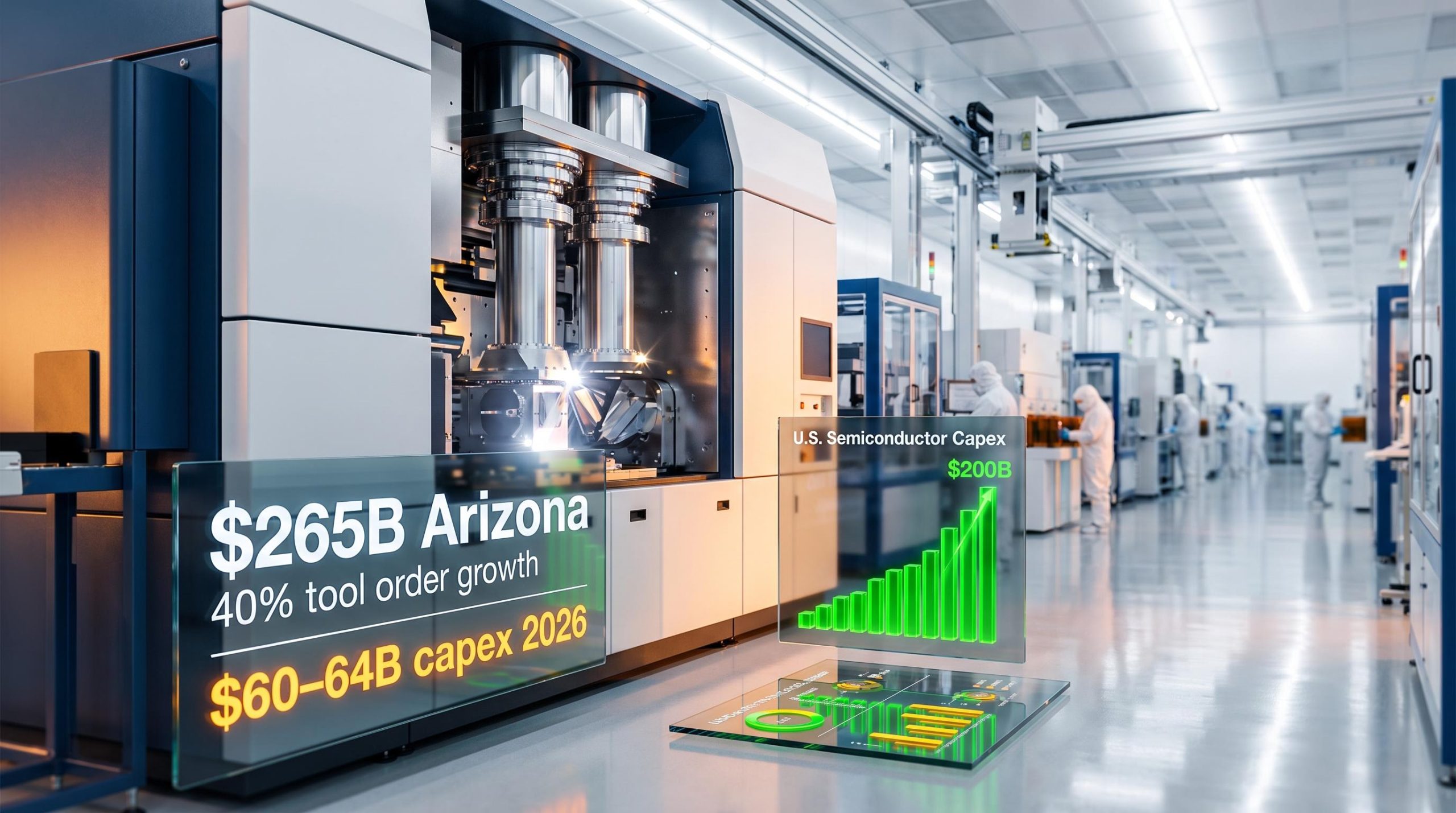
TSMC committed $265 billion to Arizona. Intel increased tool purchases by 40% in a single year. Tesla broke ground on a semiconductor fab of its own. These are not routine capital expenditure updates. They are the opening moves of the largest concurrent buildout of chip manufacturing capacity the United States has ever attempted.
Three separate demand streams are converging in the same two-year window: TSMC’s AI-driven fab expansion, Intel’s foundry programme across four states, and Tesla’s Terafab initiative in Texas. The CHIPS and Science Act, with more than $52 billion in federal incentives, is designed to amplify each of these commitments, not replace them. The combined capital flowing into U.S. semiconductor infrastructure dwarfs anything a single company or a single policy could produce alone.
Here is what the spending actually tells you about where U.S. chip infrastructure stands right now, which companies and supply chain layers are absorbing the capital, why equipment makers sit at the centre of this cycle, and what the back-end packaging gap means for whether reshoring is genuinely complete or still half-built.
A capex supercycle unlike anything the semiconductor industry has seen
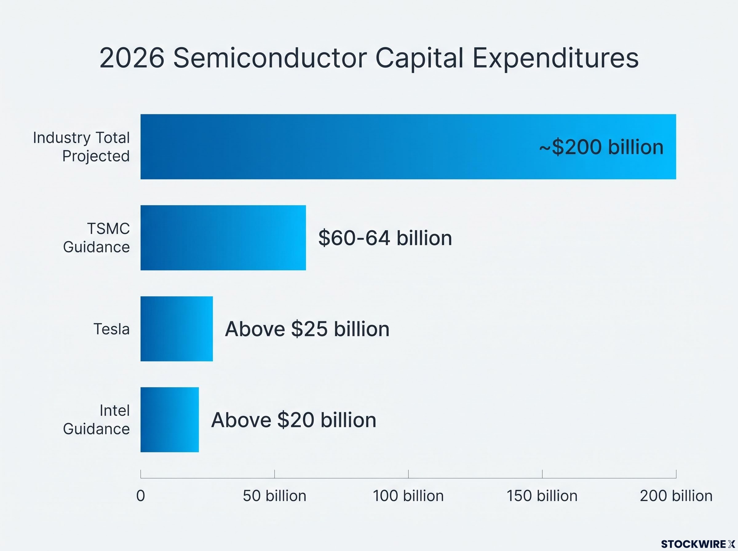
Industry estimates suggest semiconductor capital expenditure reached approximately $166 billion in 2025 and is projected to approach $200 billion in 2026, a roughly 20% year-over-year increase. That growth rate spans both foundry and memory segments, which means equipment demand pressure is distributed across the entire supplier base rather than concentrated at one customer.
What distinguishes this from a normal capex upturn is the simultaneous presence of three conditions:
- Simultaneous commitments: Multiple companies building or expanding fabs at the same time, not sequentially
- Policy amplification: The CHIPS Act’s incentives are crowding in private capital, enlarging project scopes beyond what companies would fund unilaterally
- AI-driven demand pull: Artificial intelligence workloads are creating a structural floor under chip demand that is independent of the traditional consumer electronics cycle
The CHIPS and Science Act channels more than $52 billion in U.S. incentives into fabs, advanced packaging, and research, explicitly designed to accelerate private investment and strengthen domestic supply chain resilience.
NIST’s CHIPS Act incentive breakdown allocates $39 billion for fabrication incentives and $3 billion specifically for the National Advanced Packaging Manufacturing Program, confirming that the federal commitment extends explicitly to back-end supply chain gaps, not only front-end wafer production.
The policy commitments made in 2022-2023 are now materialising as verified, large-scale private capital deployment. This is the translation phase.
When big ASX news breaks, our subscribers know first
TSMC’s Arizona bet reaches $265 billion as AI demand rewrites the capex calculus
TSMC lifted its 2026 capex guidance to $60-64 billion, moving up from a prior level of around $56 billion. The company cited two factors behind the increase: unexpectedly robust AI demand and elevated semiconductor equipment costs. That second factor matters enormously. It tells you that the tools required to manufacture leading-edge chips are becoming scarcer and more expensive, which directly benefits equipment makers’ pricing power before volume growth is even counted.
The $770 billion in projected 2026 hyperscaler capex is compressing return on equity among the largest technology companies while simultaneously creating structural pricing power for the semiconductor suppliers receiving those orders, a dynamic that explains why rising equipment costs function as a revenue tailwind rather than a margin headwind for tool makers.
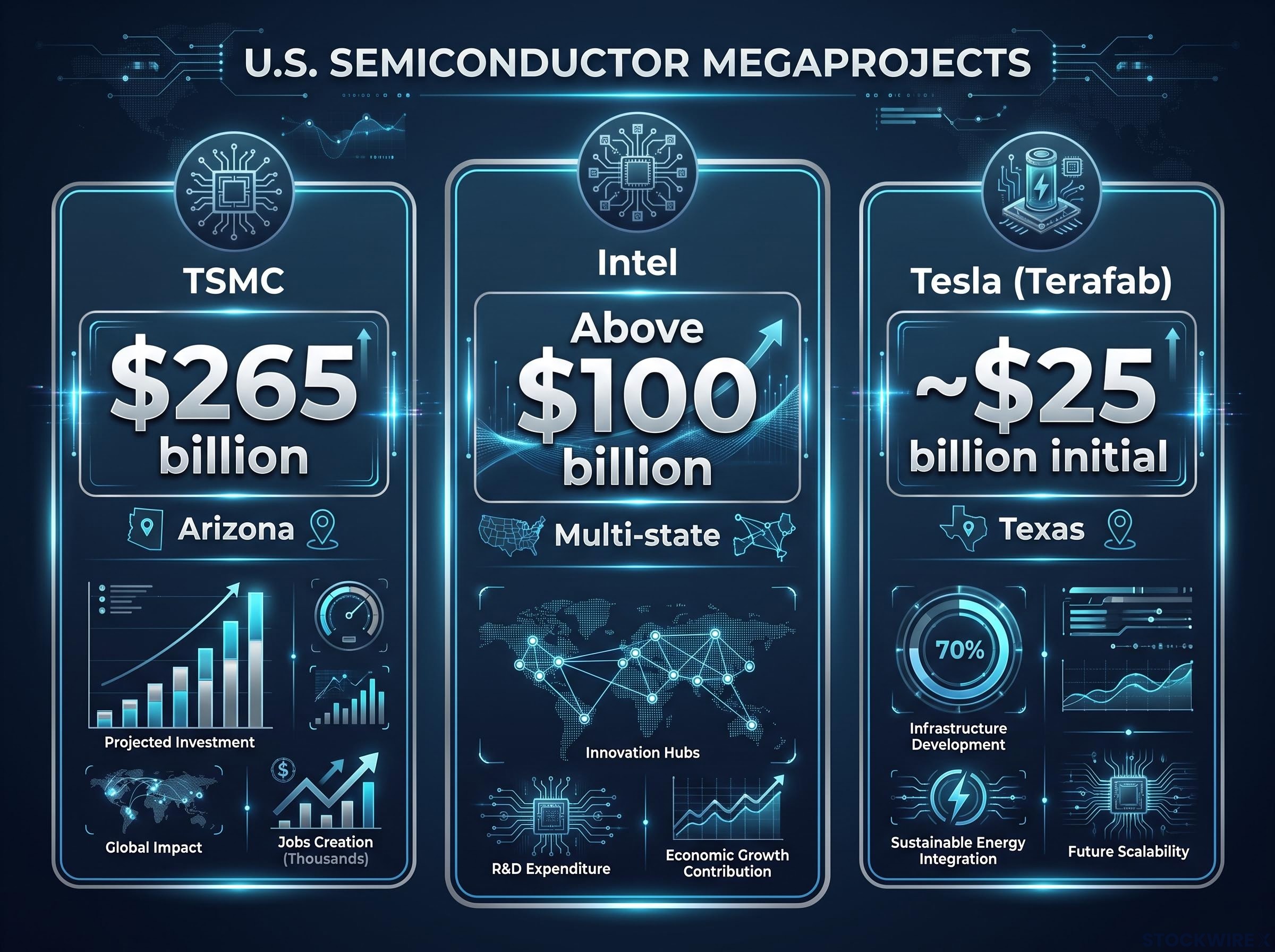
TSMC has separately committed a further $100 billion to its Arizona build, taking the total U.S. investment at that site to $265 billion and encompassing around four new fabrication facilities.
| TSMC capex metric | Value | Primary driver |
|---|---|---|
| Prior 2026 guidance | ~$56 billion | Planned node expansion |
| Current 2026 guidance | $60-64 billion | AI demand surge and rising equipment costs |
| Total Arizona commitment | $265 billion | Full-scale U.S. reshoring of leading-edge capacity |
What analysts say rising equipment costs signal
TSMC’s own attribution of equipment costs as a capex driver is not a one-quarter pressure. It reflects a structural reality at leading-edge nodes: the tools are more complex, scarcer, and more expensive with each generation. Citi analysts explicitly characterised the higher capex guidance as bullish for semiconductor equipment suppliers, noting that the step-up is heavily driven by tool purchases rather than construction budgets. That distinction matters because it means the capital is flowing directly into equipment order books.
Intel’s tool orders jump 40% as its multi-state factory programme moves from announcement to installation
Year-over-year, Intel’s tool procurement expanded by roughly 40%. That figure is the most direct evidence available that this capex cycle is creating productive capacity, not just groundbreakings and press releases. Tools being installed in fabs mean wafers will follow.
Intel’s 2026 capex guidance was revised upward to above $20 billion from a prior level of around $18 billion. Beyond that, the company has indicated that 2027 spending will be “meaningfully greater” than 2026, with the bulk of investment directed at U.S. manufacturing sites. That commitment extends equipment demand visibility well beyond a single fiscal year, which is unusual for an industry historically defined by sharp cyclical swings.
The programme spans four U.S. states:
- Arizona: New leading-edge fabrication facilities
- New Mexico: Advanced packaging capacity, including Foveros 3D stacking
- Oregon: Existing site expansion and process development
- Ohio: New fab construction for future node production
Intel has reportedly received up to approximately $8 billion in CHIPS Act grants, according to industry estimates. The majority of planned investment is U.S.-based.
Intel’s CHIPS Act funding confirmation from the company’s own newsroom places the direct federal award at up to $7.86 billion, a figure that refines industry estimates and underscores the scale of public-private capital co-investment flowing into Intel’s multi-state manufacturing programme.
Intel has communicated that 2027 capital expenditure will be “meaningfully greater” than 2026, suggesting a multi-year ramp tied to its foundry ambitions and its effort to regain process leadership.
The 40% tool purchase figure matters more than the headline capex number because it measures what is actually being installed in fabs right now, giving equipment makers confirmed revenue rather than projected demand.
What Terafab is and why Tesla’s semiconductor ambitions matter beyond electric vehicles
Tesla has put its 2026 capital expenditure at above $25 billion, with spending expected to keep rising across the following two to three years. A portion of that spending flows into Terafab, Tesla’s semiconductor manufacturing initiative located in Texas, targeting AI computing capacity.
Elon Musk’s stated goal is a facility capable of producing one terawatt of AI compute per year. To put that in perspective, analysts estimate that output would represent roughly 70% of TSMC’s current total worldwide production from a single site. That is an extraordinary ambition.
Musk’s target of one terawatt of annual AI compute production would, if realised, require processing tens of millions of advanced logic wafers annually, implying tool requirements across lithography, etch, deposition, inspection, and packaging that would rival the largest fabs operating today.
The verified figures and the projections need to be clearly separated:
- Phase one (verified): Initial capex target of approximately $25 billion, as stated by Tesla and Musk, covering site construction and early tool installation
- Phase two (projected): Industry analysts estimate total investment could scale to $55-119 billion over multiple years, though these figures remain unconfirmed
- Phase three (aspirational): Full one-terawatt annual production, which would require tooling, workforce, and supply chain buildout that no single-site fab has attempted
Even if Terafab develops in stages over many years, its existence as a committed project adds a third independent demand stream for leading-edge fab equipment. That reduces the equipment market’s dependence on the TSMC-Intel duopoly and broadens the addressable order base for suppliers.
Closing the loop on reshoring: why advanced packaging is the missing half of domestic chip supply chains
Advanced packaging refers to techniques such as chip stacking, high-density interconnects, and multi-chip module assembly, where multiple chip components (called dies) are combined into a single package that performs as one unit. For AI accelerators, this step is where final performance gains are unlocked, because tightly integrating GPU, memory, and networking dies reduces the distance signals travel and cuts power consumption.
Historically, most advanced packaging capacity has been concentrated in Asia. That means even when front-end wafer fabrication is reshored to the U.S., the chips still need to travel offshore for packaging, a supply chain vulnerability that undermines the strategic purpose of domestic fabs.
TSMC’s CoWoS packaging yield exceeds 98% against Intel’s competing EMIB-T pilot yield of 80%-85%, a gap that sits at the intersection of front-end process leadership and back-end packaging capability and explains why reshoring advanced packaging is strategically inseparable from reshoring wafer fabrication.
Two investments are now addressing that gap directly.
| Company | Deal value | Technology focus | Strategic purpose |
|---|---|---|---|
| Amkor-Nvidia | $1.5 billion | Advanced packaging for AI accelerators | Domestic back-end capacity for Nvidia’s GPU supply chain |
| Intel | More than $4 billion | Foveros 3D stacking | U.S.-based advanced packaging at scale |
The Amkor-Nvidia partnership includes an upfront prepayment structure, meaning Nvidia is funding Amkor’s capacity build directly. That is a stronger signal of demand certainty than a standard long-term supply agreement. Nvidia is so confident in its domestic packaging need that it is willing to bankroll the buildout.
Intel’s Foveros investment in New Mexico
Foveros 3D stacking is Intel’s technology for vertically stacking multiple chip dies on top of each other, reducing the physical distance between components to cut latency and power consumption. Intel is investing more than $4 billion in New Mexico to scale this capability, directly filling a major gap in U.S. back-end infrastructure. Together with the Amkor-Nvidia deal, this marks the beginning of a domestic advanced packaging ecosystem.
The equipment suppliers absorbing this demand and how durable the cycle looks
Four companies sit at the centre of this demand wave, each serving a distinct part of the fabrication process:
- ASML: Lithography systems, including extreme ultraviolet (EUV) tools that pattern the smallest features on leading-edge chips
- Applied Materials: Deposition and etch equipment that builds and shapes the layers of a chip
- Lam Research: Etch and deposition tools, particularly for memory and advanced logic
- KLA: Metrology and inspection systems that detect defects and verify manufacturing precision
With TSMC, Intel, and Terafab all in simultaneous expansion phases, these suppliers face demand from multiple independent order sources at once. That reduces the single-customer concentration risk that has historically made equipment cycles volatile.
Two data points capture the tool intensity of this cycle most precisely. Intel’s 40% year-over-year tool purchase growth confirms that productive capacity is actively being installed. TSMC’s attribution of rising equipment costs as a capex driver confirms that tool scarcity and unit value are both increasing. Both signals point in the same direction: capital is flowing heavily into equipment order books.
The durability question is real. One reading is structural: AI demand pull is independent of policy and creates its own investment logic that persists regardless of incentive windows. The alternative reading is that these commitments are concentrated in a favourable CHIPS Act window that may not persist through the next political cycle.
Semiconductor equipment stocks respond primarily to capex commitment timing rather than to the end-market price cycles that drive memory, a structural distinction that has produced divergences of more than 49 percentage points between the two sub-sectors across a single cycle.
The answer likely depends on which force proves stronger: the policy-window concentration of activity, or the AI demand pull that would justify investment even without subsidies. That distinction is the defining question for U.S. semiconductor equipment spending over the next decade.
What the spending wave actually builds, and what it does not yet resolve
The verified commitments covered in this article represent a full-stack reshoring effort: wafer fabrication (TSMC, Intel), advanced packaging (Amkor, Intel New Mexico), and AI-compute manufacturing (Terafab) all being sited on U.S. soil simultaneously.
| Company | Commitment value | Focus area | Status |
|---|---|---|---|
| TSMC | $265 billion | Leading-edge fab (Arizona) | Verified |
| Intel | Above $100 billion (multi-state) | Fab and packaging | Verified |
| Intel (New Mexico) | More than $4 billion | Advanced packaging (Foveros) | Verified |
| Amkor-Nvidia | $1.5 billion | Advanced packaging | Verified |
| Tesla (Terafab) | ~$25 billion initial | AI compute manufacturing | Stated figure |
The combination of front-end fab, advanced packaging, and AI compute manufacturing all being committed simultaneously is what makes this cycle structurally different from prior reshoring efforts that addressed only one layer at a time. Whether it proves durable depends on three leading indicators worth watching:
- Equipment order backlogs: Whether Applied Materials, Lam Research, KLA, and ASML report sustained multi-quarter backlog growth or signs of order plateauing
- CHIPS Act disbursement pace: Whether federal incentive funds flow on schedule or face delays that slow private capital deployment
- Terafab groundbreaking confirmation: Whether Tesla’s semiconductor initiative moves from stated ambition to confirmed construction milestones
The central unresolved question is whether this investment yields durable domestic capability, including U.S.-based tool and materials suppliers, or represents a concentration of activity in a single favourable policy window. The spending commitments are verified. The structural permanence is not.
For investors seeking a disciplined framework to act on these signals, our dedicated guide to semiconductor cycle investing covers the five-indicator system for capturing peak-cycle gains without holding premium multiples past the point where the 2027-2029 supply wave begins compressing returns.
This article is for informational purposes only and should not be considered financial advice. Investors should conduct their own research and consult with financial professionals before making investment decisions. Financial projections referenced in this article are subject to market conditions and various risk factors. Statements regarding future capital expenditure plans are forward-looking and subject to change based on market developments and company performance.