Dorsavi Clears Key Manufacturing Hurdle Putting 22nm Memory Chip on Track
dorsaVi clears the key materials hurdle on its path to 22nm RRAM commercialisation
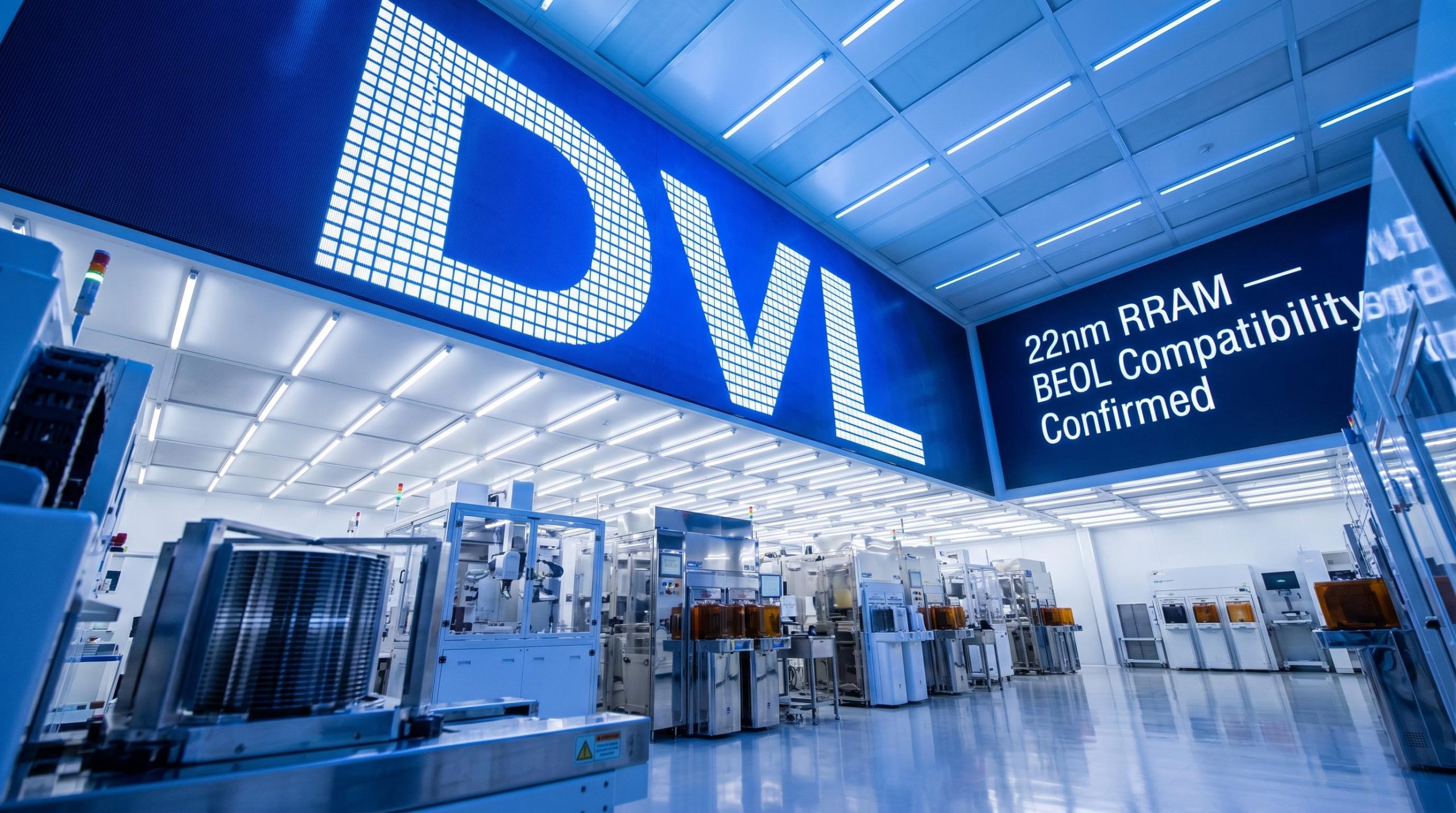
dorsaVi Limited (ASX: DVL) has announced a significant dorsaVi 22nm RRAM commercialisation milestone, with three RRAM material stacks successfully passing commercial foundry Back-End-of-Line (BEOL) compatibility testing. Qualifying three distinct stacks rather than one reduces single-stack risk and gives the engineering team flexibility when selecting the final production stack. The result removes the principal technical risk from the program and positions the company to manufacture RRAM on standard commercial CMOS production lines at scale, with a 180nm tape-out targeted for Q3 2026 and the 22nm design phase commencing H2 2027.
What just changed — and why it matters
Prior to this milestone, materials compatibility represented the primary bottleneck in the program. With BEOL qualification now complete across all three stacks, the manufacturing path is de-risked and foundry-ready. Key outcomes from the announcement include:
- Three material stacks qualified against BEOL compatibility standards
- All three integrate with existing commercial CMOS processes, with no bespoke facility required
- Pre-tape-out work, including circuit and layout designs, is complete; formal design review is scheduled for June 2026
- Tape-out at a Tier-1 commercial foundry is targeted for Q3 2026
- 22nm design phase commencing H2 2027
Mathew Regan, Group Chief Executive Officer, dorsaVi
“Qualifying three RRAM stacks against commercial foundry standards was the principal technical hurdle in this program, and it is now behind us. BEOL compatibility means we can manufacture on existing CMOS production lines rather than a dedicated facility, which is what supports the unit economics required for production volume. The team is focused on tape-out at a Tier-1 commercial foundry in Q3 2026, with the 22nm design phase commencing in the second half of 2027. For our sensor business, this is the platform that allows our existing FDA-cleared devices to evolve from streaming sensors into local inference nodes.”
When big ASX news breaks, our subscribers know first
Understanding RRAM and why BEOL compatibility is the commercial gating factor
Resistive Random Access Memory (RRAM) is a high-endurance, low-power, non-volatile memory technology that enables in-memory computing for edge devices. In semiconductor manufacturing, a “stack” refers to the vertical arrangement of thin-film material layers, typically a switching medium sandwiched between electrodes, that forms each individual memory cell.
BEOL (Back-End-of-Line) compatibility is the commercial gating test for any RRAM program. RRAM layers must survive standard foundry thermal budgets and chemical processes without degrading the silicon beneath. Without this compatibility, a company is forced to build or commission a dedicated facility, an approach that destroys the unit economics required for high-volume production.
Three parameters determine whether an RRAM stack is commercially viable:
- Scalability (Foundry Fit): The stack must use standard deposition and etching tools already present in high-volume foundries
- Integration (CMOS Compatibility): Materials must survive the foundry’s thermal budgets and chemical etching processes without degradation
- Performance (Application Target): Material composition is optimised for write voltage, endurance, and uniformity for specific target sectors
dorsaVi has now cleared all three parameters across all three stacks. This is the result that bridges RRAM’s theoretical promise and high-volume commercial production.
What the technical data confirms
| Development Milestone | Technical Achievement | Commercial Impact |
|---|---|---|
| Low-Power Operation | Stable sub-1V DC switching demonstrated across all three qualified stacks | Meets the low-voltage requirement for battery-powered and energy-harvesting edge devices |
| Process Qualification | Three testing phases closed: etch study, particle scan, and BEOL compatibility short-loop | Confirms process cleanliness and manufacturing stability using standard foundry tools |
| Simulation Readiness | Cell variation characterised and integrated into the circuit simulation environment | Gives engineering teams the data to model real-world performance and yield |
| Path to Integration | BEOL thermal budget met; stacks ready for 1T1R integration and AC testing | Moves the project from materials testing into functional memory array development |
The leap to 22nm — unlocking high-value commercial markets
The transition from the 180nm validation node to the 22nm primary commercial target represents a generational step in capability. The 22nm node delivers higher cell density, lower energy per operation, and improved thermal robustness compared with the 180nm test vehicle.
For dorsaVi’s existing revenue-generating sensor business, this scaling carries direct strategic weight. It is what brings exoskeletons, prosthetics, medical implants, and industrial robotics into commercial scope, enabling the company’s existing FDA-cleared sensors to evolve from raw-data streaming devices into autonomous, on-body inference nodes. The announcement explicitly maps the hardware gains of the 22nm node to its highest-potential commercial sectors:
| Target Sector | Key Technical Gain at 22nm |
|---|---|
| Battery-powered edge devices (medical implants, wearables, IoT) | 20–30% reduction in write voltage; lower energy cost per operation |
| High-speed sensors and AI compute (exoskeletons, on-body inference) | More than 2× increase in cell density; endurance above 10 million program/erase cycles |
| Industrial robotics | Data retention above 10 years at 125°C; 40°C improvement in thermal robustness over previous baselines |
Compute-in-Memory — eliminating the Memory Wall
Design and layout work is complete for a Compute-in-Memory (CIM) macro integrated directly onto the 256Kb RRAM array. By executing neural network inference within the memory fabric itself, the architecture overcomes the “Memory Wall”, the industry-wide bottleneck where 70%–90% of compute energy is typically wasted moving data between separate processors and external memory.
The CIM layer is designed to integrate with dorsaVi’s proprietary neuromorphic IP portfolio, including delta-sigma neurons, memristive learning arrays, and adaptive neural converters. When applied to wearable robotics, exoskeletons, and autonomous systems, the architecture is projected to deliver:
- Roughly one order-of-magnitude lower energy consumption per inference
- Multi-fold reduction in end-to-end decision latency, supporting sub-millisecond control loops for robotics applications
- Projected 25%–50% reduction in the number of sensors required per body
- More than double the battery life for the overall system
The next major ASX story will hit our subscribers first
Roadmap to commercialisation — what comes next
The 180nm test chip is a deliberate validation step, purpose-built to de-risk integration before scaling to the commercial 22nm node. The phased approach is designed to close the technical gap between material science and functional silicon integration before committing to the higher-value node. Sequential milestones from the announcement are as follows:
- June 2026 — Formal design review scheduled; Layout Versus Schematic (LVS) confirmed on the MAC array and test keys
- Q3 2026 — Tape-out submission to Tier-1 commercial foundry
- 2027 — Foundry processing and multiple rounds of BEOL integration with research partners
- H2 2027 — 22nm design phase commences, leveraging the validated 180nm architecture
Operational alignment across all consortium partners is maintained on a bi-weekly cadence, sustaining the technical momentum required to advance toward full commercialisation of the hardware platform.
Don’t Miss the Next ASX Tech Breakthrough
Big News Blast delivers FREE breaking ASX tech news directly to your inbox within minutes of release, complete with in-depth analysis. Join 20,000+ subscribers already staying ahead of the market. Click the “Free Alerts” button at Big News Blast to get the next major tech announcement the moment it drops.