Every generation of chip manufacturing has had one technology that determined who could reach the frontier. Right now, that technology costs more than a jumbo jet and fits inside a factory the size of a tennis court. ASML’s High NA extreme ultraviolet (EUV) lithography system, the EXE:5200, represents the first fundamental change to the optical design of chip-printing machines in over a decade. With Intel already running tools in its Oregon development lab, Samsung installing its first unit in March 2025, and UBS projecting 20-40% cost savings on critical chip layers, the technology is moving from laboratory curiosity to genuine production consideration. Yet most investors and technically curious readers have only encountered it as a line item in an analyst note. What follows builds a complete mental model of what High NA EUV actually is, why it changes the economics of advanced manufacturing, and what the adoption timeline realistically looks like across the world’s three leading chipmakers.
The problem that High NA EUV was built to solve
As chip features shrink below certain pitch thresholds, a single exposure from a standard EUV machine can no longer print them in one pass. The workaround is multi-patterning: splitting the work across multiple lithography cycles, each of which adds its own chain of process steps. At current and near-future logic nodes, multi-patterning is not an inconvenience; it is the single largest cost and throughput constraint in advanced manufacturing.
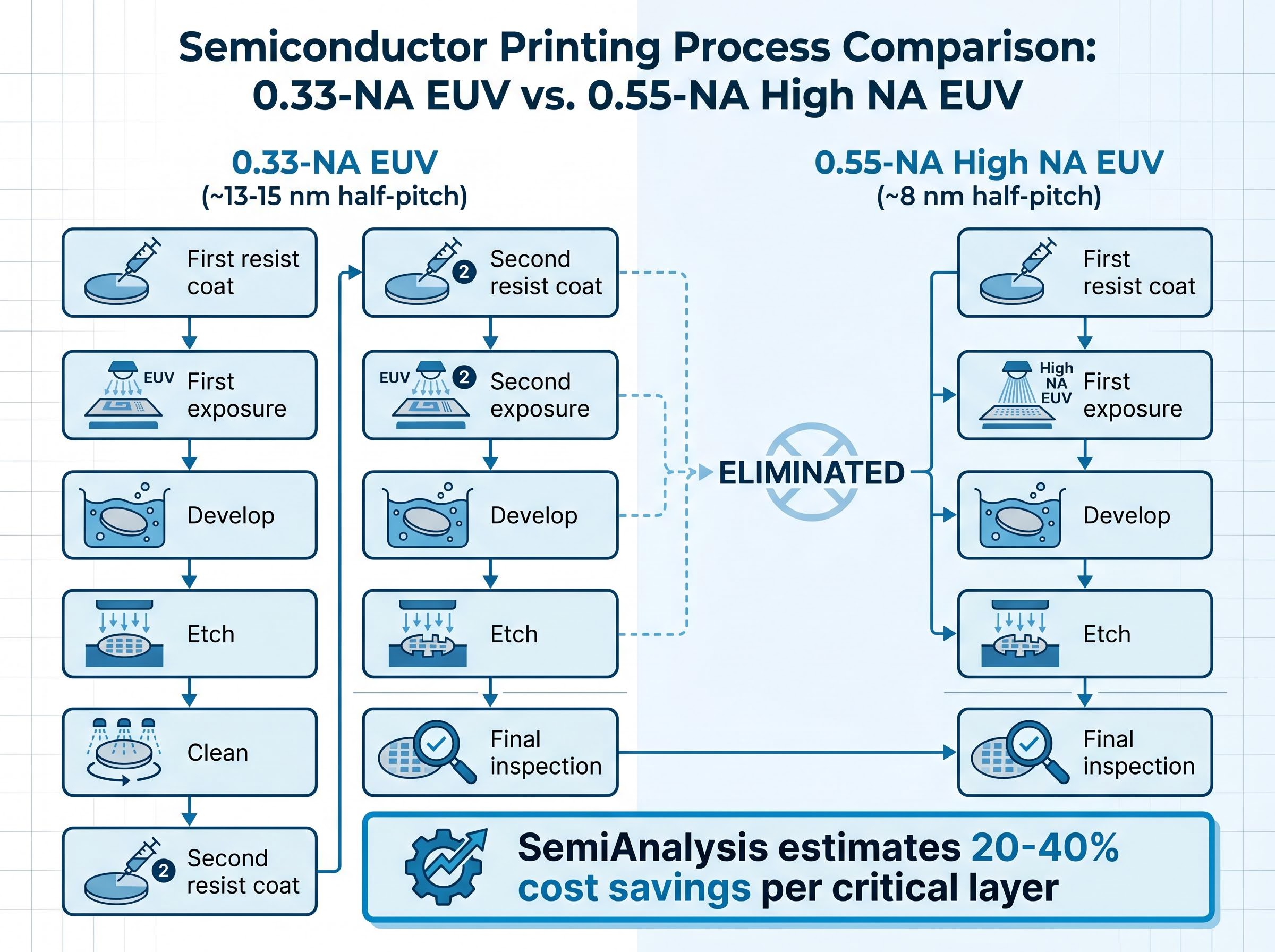
A typical litho-etch-litho-etch (LELE) double-patterning flow on a 0.33-NA EUV scanner involves:
- First resist coat
- First exposure
- Develop
- Etch
- Clean
- Second resist coat
- Second exposure
- Develop
- Etch
- Final inspection
That is two scanner passes and up to 10-12 additional process steps per critical layer. Each step costs time, consumables, and yield risk.
Why multi-patterning becomes unworkable at sub-2-nm nodes
The problem compounds at the smallest feature sizes. The practical single-exposure resolution limit of a 0.33-NA EUV system sits at approximately 13-15 nm half-pitch. At post-2-nm logic nodes, some layers require triple patterning to reach the target pitch, and every additional patterning step introduces overlay tolerances that stack. Alignment errors accumulate across passes, degrading yield at precisely the features where dimensional control matters most.
The throughput ceiling tightens in parallel. Atomic layer deposition (ALD) based multi-patterning steps, a common technique for the most demanding layers, are bottlenecked at approximately 30 wafers per hour. Financial cost per layer scales roughly with patterning count, meaning triple-patterned layers are inherently the highest-cost layers in any advanced logic chip. The industry needed a way to print finer features in a single pass. High NA EUV was built to be that answer.
When big ASX news breaks, our subscribers know first
What 0.55-NA optics actually change about the physics of printing
On a spec sheet, the change looks like a single number: numerical aperture (NA) rising from 0.33 to 0.55. The physics behind that number determines whether the economic claims about High NA hold up.
Numerical aperture measures a lens system’s ability to gather light and resolve fine detail. A larger NA means the lens collects light from wider angles, allowing it to distinguish smaller features on the wafer surface, in much the same way a camera lens with a wider aperture gathers more light to produce a sharper image. Moving from 0.33 to 0.55 improves theoretical resolution proportionally, enabling single-exposure printing of features that previously required double or triple patterning.
The trade-off is field size. High NA optics produce a smaller exposure area per shot, which ASML compensates for with higher source power and improved stage throughput to maintain competitive wafer-per-hour rates.
“0.55-NA systems can support approximately 8 nm half-pitch single exposure, versus approximately 13-15 nm for 0.33-NA machines, the gap that forces multi-patterning at today’s most advanced nodes.”
The resolution gain is not incremental. It is the difference between printing a layer once and printing it two or three times.
ASML’s EXE:5200B specifications confirm the 0.55-NA system delivers approximately 8 nm resolution, printing features 1.7 times smaller than the prior generation, with projection optics co-developed with ZEISS SMT to achieve the optical performance gains the architecture requires.
| Parameter | 0.33-NA EUV | 0.55-NA (High NA) EUV |
|---|---|---|
| Practical single-exposure half-pitch | ~13-15 nm | ~8 nm |
| Typical patterning at post-2-nm logic | Double or triple patterning | Single exposure |
| Effective layer throughput | Constrained by multi-pass flows | Single-pass; >100% effective gain vs multi-patterning |
How the economics change when you remove a patterning step
The cost comparison between High NA and multi-patterning is not a simple tool-price calculation. A High NA EXE:5200 system costs approximately €350-400 million, roughly 1.5 times the price of a latest-generation 0.33-NA scanner in the low-to-mid €200 million range. On capex alone, the premium looks steep.
The arithmetic shifts when the full process cost of the eliminated steps enters the equation. Replacing a double-patterning flow with a single High NA exposure removes the second scanner pass, resist coat, develop, etch, and inspection. That elimination is described as equivalent to more than doubling effective throughput at the layer level: approximately 80% improvement versus LELE flows and more than 100% versus the most complex multi-patterning alternatives.
SemiAnalysis estimates 20-40% cost savings per critical layer when High NA replaces triple-patterned 0.33-NA/DUV flows at the most aggressive logic layers. IBS analysts project a 10-20% reduction in cost per transistor at post-2-nm nodes when High NA is applied selectively to the densest layers.
“Eliminating the second exposure, resist coat, develop, etch, and inspection steps leads to more than 100% effective throughput improvement at the layer level.”
| Scenario | Tool capex per layer | Process steps | Effective throughput | Relative cost index |
|---|---|---|---|---|
| 0.33-NA single exposure (where applicable) | Baseline | Single pass | Baseline | 1.0 |
| 0.33-NA double patterning | ~2× baseline | 10-12 additional steps | ~50% of baseline | ~2.0-2.5 |
| High NA single exposure | ~1.5× baseline | Single pass | >2× vs double patterning | ~0.6-0.8 |
The cost-per-layer economics at advanced nodes directly determine chipmaker margins and the pace at which fabs adopt new equipment. For ASML, each additional tool acceptance translates into revenue that compounds across a customer base with no alternative supplier for this capability.
Where the world’s leading chipmakers actually stand today
Three companies have the process technology and capital to deploy High NA EUV. Each has chosen a different pace, and each position reflects a rational response to the same technology.
Intel is the confirmed first mover. The EXE:5200B passed acceptance tests in December 2025 at the company’s Hillsboro, Oregon D1X facility. Intel frames High NA as central to its 14A node development in the second half of the decade, while the current 18A programme does not depend on it. The tool is in development and pathfinding use, not high-volume manufacturing.
Samsung installed its first High NA tool, an EXE:5000, at the Hwaseong Campus in March 2025 for R&D and evaluation. Production-oriented EXE:5200B units are targeted for a 2026 ramp, beginning with the 1.4-nm generation. Samsung’s approach balances ambition with a recognition that 0.33-NA and multi-patterning will dominate its near-term nodes.
TSMC has made no confirmed installation as of May 2026. CEO C.C. Wei has stated that High NA will be deployed “when the cost and maturity make sense for customers,” with adoption expected at A14P or later. The company’s N2 and A14 nodes rely on 0.33-NA EUV, a deliberate choice to let the ecosystem mature before committing capital.
TSMC’s manufacturing lead at 3nm rests on a capacity gap that makes the company’s wait-and-see posture on High NA EUV a deliberate choice rather than a constraint; the company is targeting approximately 180,000 wafers per month at that node by end-2026, roughly eight times the estimated output at both Samsung and Intel combined.
| Chipmaker | Current High NA status | First planned HVM node | Expected HVM timeline |
|---|---|---|---|
| Intel | EXE:5200B accepted Dec 2025; R&D use | Intel 14A | Second half of decade |
| Samsung | EXE:5000 installed Mar 2025; R&D | 1.4-nm generation | Production ramp planned 2026 |
| TSMC | No confirmed installation | A14P or post-A14 | Deferred; no confirmed dates |
Three barriers shape the pace for all three:
- Tool cost and capex intensity: At €350-400 million per system, each installation is a significant capital commitment gated by expected wafer volume.
- Mask and resist ecosystem maturity: New resist chemistries and mask-writing capabilities must reach production quality before High NA tools can run at scale.
- Overlay and focus control requirements: The tighter tolerances at 0.55-NA demand new metrology and process control infrastructure that fabs are still qualifying.
Why no competitor can replicate what ASML has built
Nikon has effectively ceded the leading-edge EUV and High NA market to ASML, concentrating instead on ArF immersion and DUV productivity improvements. The company has no announced High NA EUV programme. Canon promotes nanoimprint lithography (NIL) as a lower-cost alternative for certain memory and specialty applications, but defect density and overlay limitations prevent NIL from displacing High NA EUV at logic nodes below 2 nm.
- ASML: Sole provider of EUV and High NA EUV lithography; no announced competitor in the segment
- Nikon: Focused on ArF immersion and DUV; no High NA programme announced
- Canon: NIL approach viable for select memory applications; defect and overlay challenges preclude use at sub-2-nm logic
Analysts at EE Times concluded in May 2025 that ASML’s High NA technology “cements its monopoly” at the leading edge, with Nikon and Canon non-participants in the segment. No credible High NA EUV competitor exists on the horizon as of May 2026.
The ecosystem effect that makes the gap self-reinforcing
The moat extends beyond the scanner itself. Resist chemistry, mask-writing tools, metrology hardware, and process integration knowledge are all co-developed around ASML’s platform. The cost of switching to a competitor, if one existed, would involve rebuilding the entire supporting stack.
IMS Nanofabrication and other mask-side firms are building toward High NA mask requirements, further deepening integration around ASML’s roadmap. Mask complexity and cost will rise with High NA, creating adjacent ecosystem opportunities but no competing lithography platform. The competitive position is not merely a lead; it is a structural condition shaped by decades of co-investment between ASML, its customers, and a specialised supply chain that has no reason to duplicate itself for a second entrant.
The next major ASX story will hit our subscribers first
The technology tailwind is real, but the ramp will reward patience
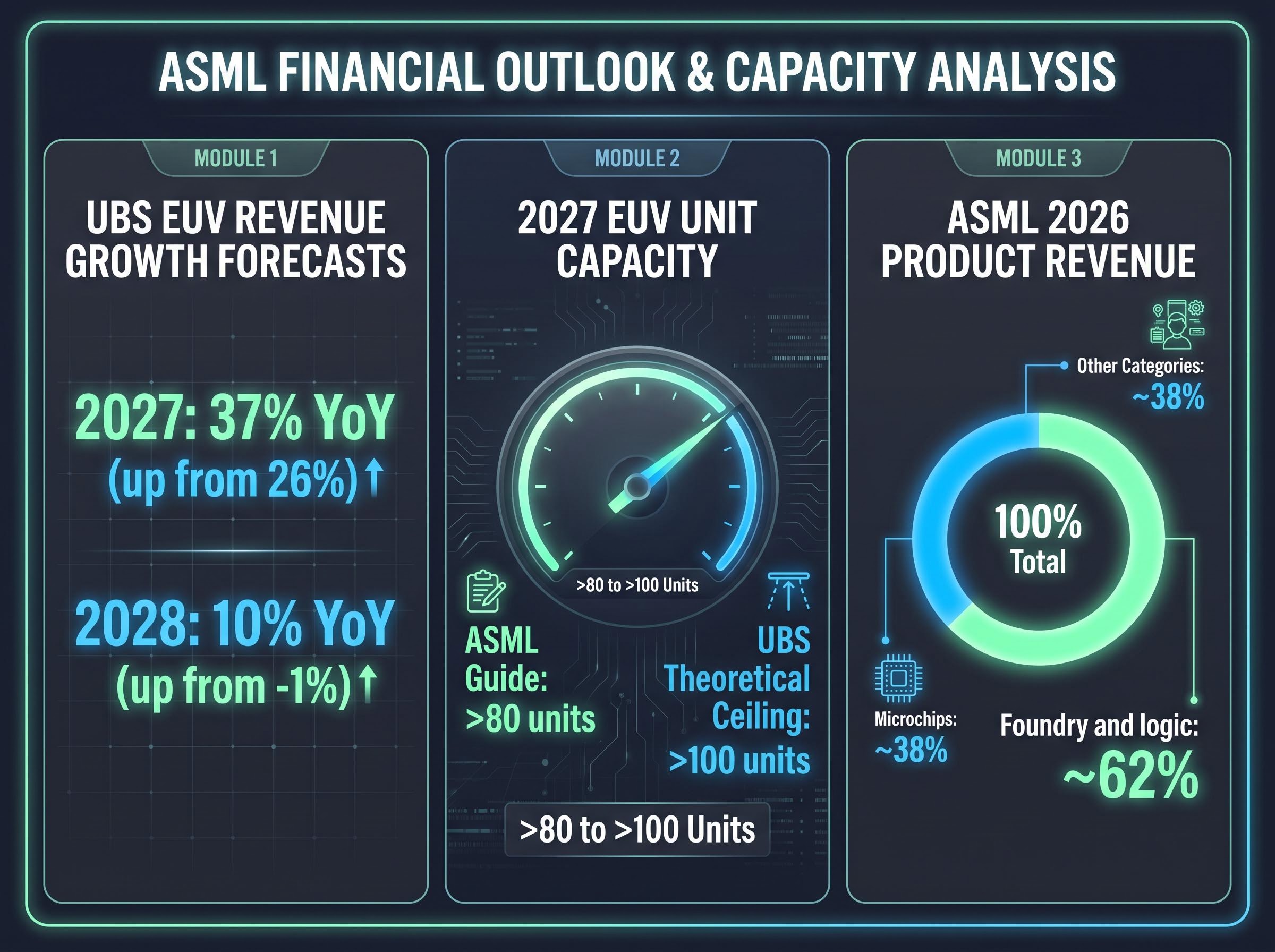
UBS expects broad chipmaker adoption within 2-3 years from mid-2026, driven by the 20-40% cost savings case becoming increasingly compelling as node complexity increases. The firm raised its EUV revenue growth forecast for 2027 to 37% year-over-year (from a prior 26% estimate) and revised its 2028 projection to 10% year-over-year (from a prior -1%). ASML has guided for capacity of more than 80 EUV units for 2027, with UBS internal analysis suggesting a theoretical ceiling above 100 units.
The near-term reality is more measured. ASML CFO Roger Dassen emphasised that widespread High NA HVM adoption is a “latter-half-of-the-decade” phenomenon, with near-term revenue contribution remaining modest.
“ASML CFO Roger Dassen emphasised that widespread High NA HVM adoption is a ‘latter-half-of-the-decade’ phenomenon, with near-term revenue contribution remaining modest.”
TrendForce consensus points to mass production around 2027-2028 for early adopters. Foundry and logic accounted for approximately 62% of ASML product revenue in 2026, framing the segment’s weight in the company’s forward trajectory.
Three sequential conditions must be met before High NA drives material revenue:
- Tool delivery and fab acceptance at scale: Physical systems must be manufactured, shipped, installed, and qualified at multiple customer sites.
- Resist and mask ecosystem readiness: New resist chemistries and mask-writing infrastructure must reach production-grade quality and yield.
- Yield learning curves reaching commercial viability: Fabs must demonstrate that High NA layers meet defect density and throughput standards for high-volume commercial output.
The technology case is strong and increasingly well-evidenced. The revenue inflection, however, is gated by delivery cadence, ecosystem maturation, and yield learning rather than demand intent. Investors who understand that gap are better positioned to evaluate ASML’s valuation and the timing of any thesis built around this technology.
Investors wanting to understand how the High NA adoption timeline translates into specific earnings forecasts will find our full explainer on the UBS ASML upgrade, which walks through the €1,900 price target rationale, the 15-20% EPS premium over consensus for 2027 and 2028, and the key risks including China export control exposure and DRAM capex cycle timing.
ASML’s valuation discount relative to U.S. semiconductor equipment peers has compressed to approximately 6-15% from a 10-year historical average of 84%, a gap that analysts at UBS argue reflects a structural mispricing of the company’s memory revenue growth and the long-term optionality embedded in High NA EUV adoption.
This article is for informational purposes only and should not be considered financial advice. Investors should conduct their own research and consult with financial professionals before making investment decisions. Past performance does not guarantee future results. Financial projections are subject to market conditions and various risk factors.
A structural shift hiding in plain sight
High NA EUV is not an incremental upgrade to existing lithography. It is a change in the optical architecture of chip printing that removes a cost floor constraining advanced node economics for years. Intel is already in development, Samsung is ramping, and TSMC will follow when the economics close. No competitor exists to offer an alternative path at these feature sizes.
Investors who understand the technology mechanism are better equipped to assess both ASML’s long-term revenue trajectory and the timeline over which current analyst optimism translates into actual earnings inflection. The question for the remainder of the decade is not whether High NA EUV will reshape advanced manufacturing economics, but how quickly the ecosystem matures to make broad high-volume adoption viable, and what that ramp looks like node by node.