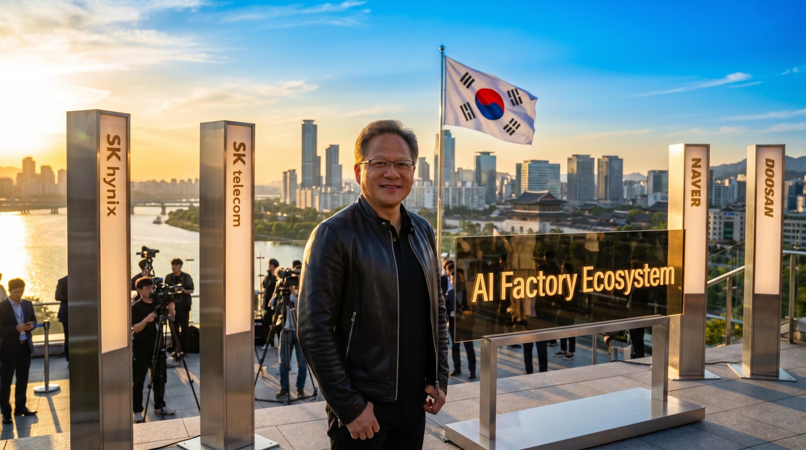
Nvidia CEO Jensen Huang arrived in Seoul on 6 June 2026 and spent two days in back-to-back meetings with senior leadership at four of South Korea’s largest technology and industrial groups. On 8 June, he announced simultaneous partnership agreements with SK Hynix, SK Telecom, Naver, and Doosan Group, spanning memory supply, gigawatt-scale cloud infrastructure, AI data centre deployment, and energy systems. Huang described the country as a linchpin for “the next decade of accelerated computing.” The agreements, none of which disclosed financial terms, represent a coordinated effort to anchor Nvidia’s AI infrastructure supply chain in a US-aligned manufacturing hub at a time when export controls are actively reshaping where AI compute capacity gets built. What follows is an explanation of each deal, why South Korea holds an outsized role in Nvidia’s global strategy, and what the combined agreements signal for the AI hardware supply chain.
What Huang announced in Seoul and why the timing matters
The four agreements were not announced in isolation. They were structured as a single coordinated package, each covering a different layer of the AI infrastructure stack. Huang met SK Group Chairman Chey Tae-won and SK Hynix CEO Kwak Noh-jung, held sessions with SK Telecom and Naver leadership, and sat down with Doosan Group executives, all within a two-day window beginning 6 June.
The unifying rationale came from Huang directly:
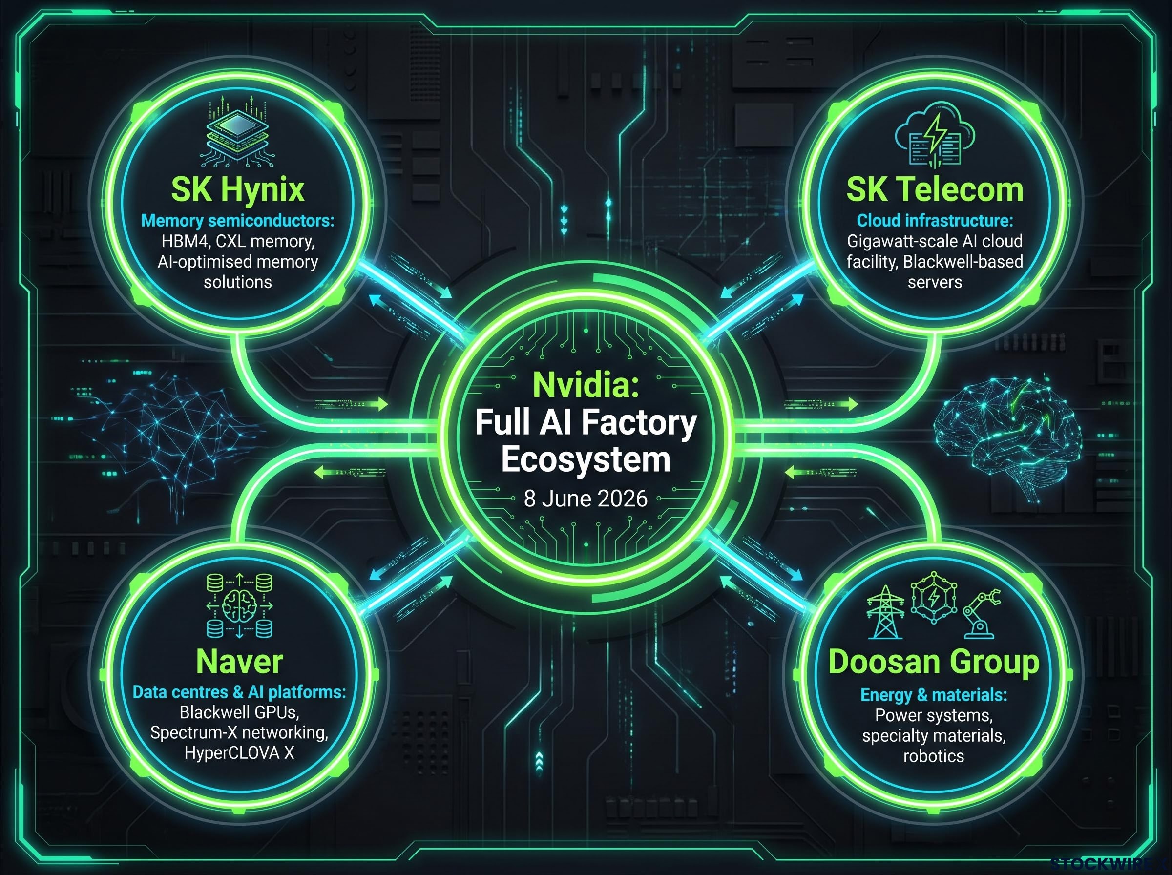
“Build a full AI factory ecosystem in Korea, from chips and memory to data centers and AI services.”
That statement frames the four partnerships not as bilateral supplier deals but as layers of a single ecosystem. The four partners and their respective roles:
- SK Hynix: Next-generation High Bandwidth Memory (HBM) and CXL memory for AI accelerators
- SK Telecom: Gigawatt-scale AI cloud facility for Korean enterprise clients
- Naver: Blackwell GPU and Spectrum-X networking deployment across domestic hyperscale data centres
- Doosan Group: Energy infrastructure, specialty materials for chip manufacturing, and physical AI applications
| Partner | Sector | Deal Focus |
|---|---|---|
| SK Hynix | Memory semiconductors | HBM4, CXL memory, AI-optimised memory solutions |
| SK Telecom | Cloud infrastructure | Gigawatt-scale AI cloud facility, Blackwell-based servers |
| Naver | Data centres and AI platforms | Blackwell GPUs, Spectrum-X networking, HyperCLOVA X |
| Doosan Group | Energy and materials | Power systems, specialty materials, robotics |
Financial terms were not disclosed by any party.
When big ASX news breaks, our subscribers know first
SK Hynix and the memory dependency at the heart of AI computing
SK Hynix is already Nvidia’s most important memory supplier. The company derived more than 80% of its HBM revenue from Nvidia in 2024, according to industry estimates, and its HBM3E yield rate reportedly reached the mid-80% range by mid-2025, helping it secure preferred supplier status for Nvidia’s H100 and H200 GPUs. SK Hynix and Samsung Electronics are collectively the world’s two largest memory chip producers.
The new agreement deepens that relationship rather than creating one from scratch. It extends cooperation into CXL memory and AI-optimised memory solutions, and gives SK Hynix a pathway into personal AI and physical AI markets, including edge devices and robotics platforms, using Nvidia technology as the enabler.
What the HBM4 transition means for Nvidia’s next accelerator generation
HBM4 is the memory standard designed for Nvidia’s post-Blackwell accelerator platforms. SK Hynix aims to begin mass production in 2026, with development targeting 16-layer stacks capable of approximately 1.6 TB/s bandwidth per stack, a substantial improvement over HBM3E. The company has been qualifying HBM4 engineering samples with Nvidia since late 2025, with volume production expected across 2026-2027.
HBM4 supplier qualifications for Nvidia’s Vera Rubin platform were confirmed by Jensen Huang on 5 June 2026, with SK Hynix estimated to hold 60-70% of initial volume allocations, Samsung holding roughly 25-30%, and Micron securing a smaller but strategically significant foothold, a distribution that reflects each company’s relative yield performance and entry timing into the qualification process.
“Korea’s memory and materials ecosystem is critical to the next decade of accelerated computing.” — Jensen Huang, Nvidia CEO
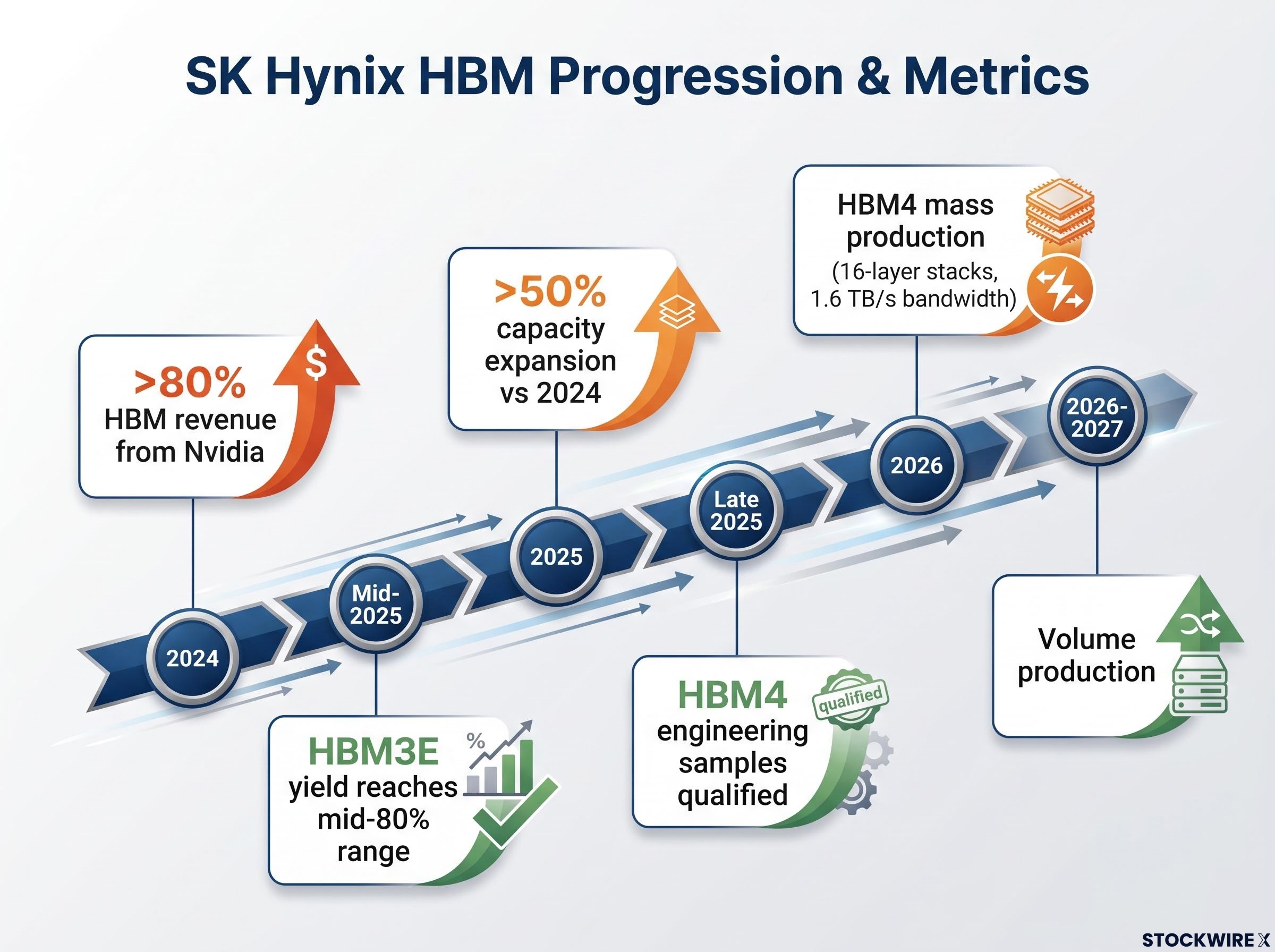
SK Hynix has also planned to expand HBM production capacity by more than 50% in 2025 compared with 2024, with trillions of won invested in expanding its Cheongju and Icheon fabrication facilities. For Nvidia, this is not a standard supplier arrangement. It is a structural dependency with limited substitution options.
The structural HBM supply constraint extends well beyond any single procurement agreement: SK Hynix projects global DRAM tightness through 2030, HBM inventory industry-wide sits at roughly 3-4 weeks, and all three major producers remain fully sold out through 2026, even as Google CEO Sundar Pichai publicly identified memory availability, not capital, as the primary limit on AI infrastructure expansion.
What HBM is and why it is not interchangeable with standard memory
The reason the SK Hynix partnership carries such strategic weight comes down to what High Bandwidth Memory (HBM) is and why it cannot simply be swapped for conventional memory chips.
GPU-based AI workloads, particularly inference tasks, are memory-bandwidth-bound. The processor can compute faster than standard memory can feed it data. HBM solves this by stacking multiple layers of DRAM vertically and mounting them directly on the same package as the GPU die, creating a short, wide data pathway that delivers far more bandwidth per watt than conventional alternatives.
Key differences between HBM and standard DDR/GDDR memory:
- Bandwidth: HBM delivers significantly higher data throughput per pin than DDR5 or GDDR6, measured in terabytes per second rather than gigabytes
- Form factor: HBM is a vertically stacked architecture bonded directly to the GPU package, not a separate module slotted into a motherboard
- Power efficiency: The shorter data pathway and wider bus reduce energy consumption per bit transferred
- Cost and complexity: HBM requires advanced packaging techniques and yields remain lower than conventional DRAM, constraining supply
Only SK Hynix, Samsung, and (to a much smaller extent) Micron produce HBM at scale. Two of those three producers are South Korean. That geographic concentration makes South Korea a supply chokepoint for the entire global AI compute industry.
SK Telecom, Naver, and the race to build sovereign AI cloud infrastructure in Korea
Two of the four partnerships address the same structural concern from different market positions: where Korean AI workloads physically run.
SK Telecom plans to construct a gigawatt-scale AI cloud facility in the Seoul metropolitan area, with an initial phase targeting operational status in 2027. The facility will use Nvidia Blackwell-based servers integrated with SKT’s A.Dot AI assistant and is designed to serve Korean manufacturing and financial sector clients.
SK Telecom has positioned itself as “Korea’s leading AI cloud carrier,” with the facility forming part of a broader global AI alliance alongside Deutsche Telekom, e&, and Singtel.
Naver’s case for keeping AI workloads inside Korea
Naver is pursuing a data-sovereignty strategy. The company’s HyperCLOVA X foundation model, which powers search, commerce, and content services, requires compute infrastructure physically located inside Korea. Under the Nvidia agreement, Naver will deploy Blackwell GPUs and Spectrum-X networking across its next-generation hyperscale data centre in Sejong and upgrades to its existing GAK data centres. The Sejong facility targets a mid-to-late 2026 operational date.
Naver Cloud is targeting Korean banks, retailers, and public sector clients, offering a regional AI platform built on domestically housed infrastructure. Both deployments are phased, with Blackwell volumes for Korean partners arriving after global hyperscaler customers, including Microsoft, Amazon, Google, and Meta, receive initial allocations.
Both deals illustrate that data-sovereignty concerns are now a structural driver of AI infrastructure investment, creating sustained domestic demand for Nvidia hardware that sits alongside, rather than competing with, hyperscaler orders.
Doosan’s role: energy, materials, and the physical infrastructure Nvidia needs
Doosan Group occupies the layer of the AI infrastructure stack that receives the least attention but imposes some of the hardest constraints. Its contribution to the Nvidia partnership spans three areas, ordered from near-term to longer-term impact:
- Materials supply: Doosan affiliates supply specialty gases, copper foils, and advanced substrates incorporated into Blackwell chip manufacturing. These materials will be qualified for current and next-generation Nvidia platforms.
- Energy infrastructure: Doosan’s micro-grid, fuel cell, and gas turbine systems are being positioned as power solutions for large-scale AI data centres. Nvidia and Doosan are collaborating specifically on high-efficiency power delivery and cooling technologies to improve data centre PUE (power usage effectiveness), a metric measuring how much total energy a facility consumes relative to the energy used by its computing equipment.
- Physical AI and robotics: Doosan’s existing robotics development work connects to Nvidia’s expanding physical AI ambitions, providing a real-world deployment pathway beyond GPU silicon.
Huang framed the energy dimension bluntly, describing future AI data centres as “electricity-hungry AI factories.” Power and materials constraints are increasingly cited by data centre operators as binding limits on expansion. Doosan’s involvement signals that Nvidia is actively working on the energy layer of its infrastructure stack, not just the silicon layer.
AI data centre power demand now runs at 3-5 times the per-rack draw of traditional cloud workloads, and the IEA projects combined data centre and AI electricity consumption will exceed 1,000 TWh by 2026, a doubling in four years that makes the energy layer of the infrastructure stack at least as constrained as the silicon layer.
South Korea’s place in Nvidia’s geopolitical supply chain map
The four partnerships share a structural logic that extends beyond any individual deal.
US export controls on advanced AI chips to China have accelerated investment in US-aligned jurisdictions. South Korea sits at the intersection of three assets no other single country currently combines: dominant HBM production through SK Hynix and Samsung, US security alignment through the US-Japan-Korea technology partnership, and robust semiconductor fabrication and grid infrastructure.
The Bureau of Industry and Security export controls on advanced computing chips, first expanded in October 2023 and subsequently tightened, explicitly target restrictions on AI hardware reaching China, creating the regulatory pressure that is actively redirecting AI compute investment toward US-aligned jurisdictions like South Korea.
Industry analysis identifies South Korea as one of three anchor geographies for AI compute capacity, alongside the US and Taiwan. Nvidia and other US chipmakers are reportedly co-locating AI data centre capacity near Korean memory fabrication facilities to reduce logistics risk and lead times. The country has been described as an AI infrastructure hub for the Indo-Pacific region.
The 8 June partnership cluster fits within this broader pattern. The agreements are consistent with a trend of US chip companies deepening ties with Korean telecoms, memory producers, and industrial groups as Washington seeks to limit reliance on mainland China for advanced semiconductor supply chains. South Korea is becoming a node in what has been characterised as a “trusted semiconductor supply chain,” particularly in memory, advanced packaging, and AI compute infrastructure.
Korea’s moment in the AI infrastructure cycle is just getting started
The four partnerships announced on 8 June 2026 are not ceremonial memoranda of understanding. They reflect structural dependencies in memory supply, cloud infrastructure, and energy systems that will take years to fully materialise. The agreements span the full AI data centre stack, from the memory bonded to GPU dies through to the fuel cells powering the facilities that house them.
Key uncertainties remain. Blackwell deployment sequencing means Korean partners will receive GPU volumes after global hyperscalers. HBM4 mass production timelines are ambitious but unconfirmed at scale. The SK Telecom facility targets 2027 operational status; Naver’s Sejong data centre aims for mid-to-late 2026.
If the “full AI factory ecosystem” model Huang described proves replicable, South Korea’s integration of memory, compute, cloud, and energy partnerships may define how Nvidia approaches other manufacturing regions. Investors and industry observers tracking these commitments should monitor SK Hynix’s HBM4 production milestones, Naver’s Sejong data centre operational date, and Nvidia’s next earnings call for any quantitative framing of the Korea partnership portfolio.
For investors tracking the Korea partnership portfolio, our full explainer on South Korean AI regulatory risk examines how a single social media post from a presidential aide in May 2026 erased more than $300 billion in market value intraday across Samsung, SK Hynix, Nvidia, and AMD before three government bodies issued coordinated denials, illustrating the speed at which non-legislative commentary can move AI semiconductor valuations.
This article is for informational purposes only and should not be considered financial advice. Investors should conduct their own research and consult with financial professionals before making investment decisions. Forward-looking statements regarding production timelines, facility completion dates, and deployment schedules are subject to change based on market developments and company performance.