Why Great Companies Can Still Be Poor Investments
2 hrs ago

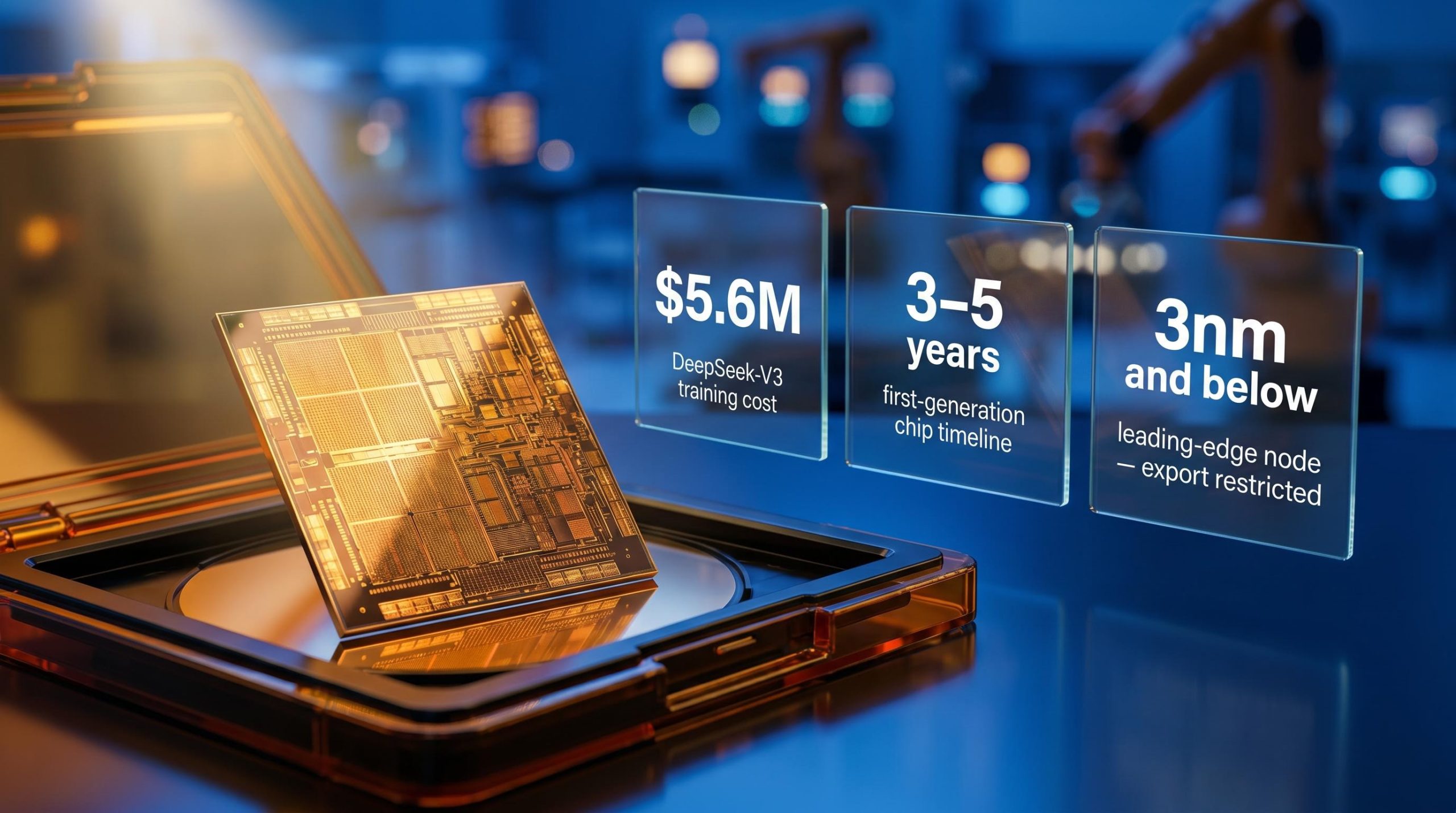
DeepSeek trained a frontier AI model for roughly $5.6 million. That figure rattled markets, reset assumptions about compute efficiency, and raised an obvious next question: if the software can be built that cheaply, why not build the chip to run it?
The answer sits at the intersection of three problems that do not behave like software problems. Semiconductor engineering operates on multi-year timelines. Fabrication capacity is concentrated in facilities governed by U.S. export controls. And the memory components that determine real-world inference speed are locked behind a separate set of supply chain restrictions. Each barrier would be formidable alone. Together, they compound.
Here is what it actually takes to go from a breakthrough AI model to competitive silicon, and why the barriers separating DeepSeek from a working chip are structural rather than merely financial. This is a working map of the problem, not a verdict on whether the company will succeed.
DeepSeek-V3 cost approximately $5.576 million to train: 2.788 million H800 GPU hours at roughly $2 per hour, using a cluster of about 2,048 H800 GPUs. That efficiency came from algorithmic innovation, specifically clever choices in model architecture and training systems that squeezed more performance from existing hardware. Software responds to that kind of ingenuity.
Hardware does not. Chip development is a multi-year systems project that moves through five distinct phases, each with its own cost curve and failure modes:
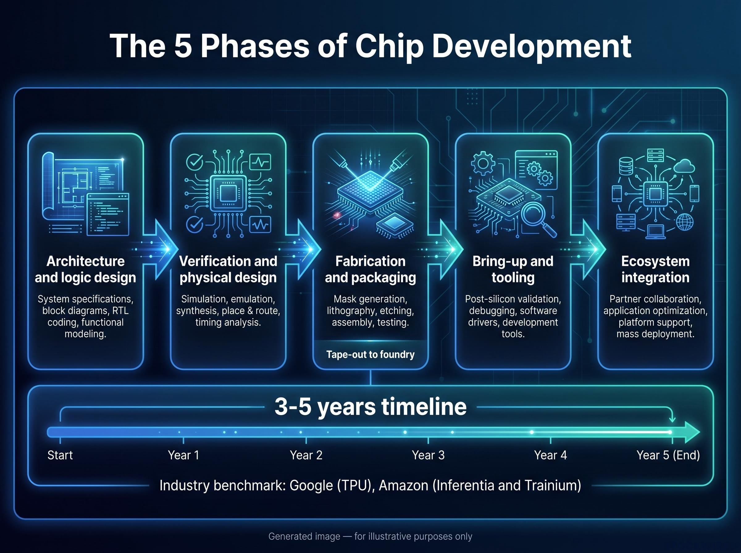
Tape-out costs at advanced process nodes run into the tens of millions of dollars per spin, and multiple spins are typically required to fix bugs and tune performance.
Industry experience from Google (TPU), Amazon (Inferentia and Trainium), and multiple AI chip startups points to a typical timeline of 3-5 years from serious project initiation to reliable high-volume production. The $5.6 million training figure is not a sign that hardware is the easy next step. It is the contrast that shows how different the two disciplines are. Mask sets, foundry tape-outs, and verification do not compress the way training budgets do. DeepSeek’s software efficiency actually makes its hardware challenge look harder by comparison, not easier.
The balance of AI compute has shifted. Training uses large GPU clusters for finite periods to build a model. Inference runs continuously, serving every user query across assistants, search tools, coding platforms, and enterprise applications. Industry observers consistently point to inference as the segment of AI hardware demand growing most rapidly, and the underlying logic is clear: the computational burden of running deployed models compounds with each additional user, each additional query, and each new product integration.
That shift opens specific design levers for chip architects. Training and inference workloads behave differently across three dimensions:
Architectures like Groq’s single-programme, multiple-data inference engines illustrate what becomes possible when you design specifically for deterministic, high-throughput inference rather than general-purpose flexibility.
DeepSeek’s models are explicitly optimised for efficient inference, emphasising low compute per token and high throughput. That means the company knows exactly which models it wants to run and how they behave under resource constraints. Knowing your workload that precisely allows hardware architects to make aggressive trade-offs, on precision support, memory hierarchy, and compute density, that a general-purpose GPU maker serving thousands of different customers cannot afford to make.
This is not theoretical. DeepSeek already demonstrated strong hardware-software co-optimisation through techniques like Mixture-of-Experts and Multi-Head Latent Attention, both of which squeeze more performance from constrained GPUs. The team already thinks at the hardware-software interface. Co-designing silicon around known workloads is more tractable than designing a general-purpose accelerator, and the inference focus is not a consolation prize for a company that cannot afford a training chip. It is a strategically rational scoping decision that gives any chip project a tighter target and a better chance of delivering something useful within realistic timelines.
Process nodes determine how many transistors you can pack into a given area of silicon. Smaller nodes mean more transistors per square millimetre, which translates directly into better performance per watt and better economics at datacenter scale. The most capable AI accelerators today use leading-edge nodes (roughly 3 nm and below).
The problem for any Chinese AI firm is that leading-edge fabrication capacity is concentrated at TSMC, Samsung, and Intel Foundry, all operating under U.S. export regimes. The U.S. Commerce Department has maintained export controls since 2022-2023, using performance-threshold and whitelist mechanisms that effectively bar Chinese AI firms from accessing these foundries for high-performance parts. China’s primary domestic foundry, SMIC, is advancing but remains constrained by its inability to access ASML’s EUV (extreme ultraviolet) lithography systems, the machines required to print the finest circuit features. EUV systems are themselves under separate export controls.
The AI chip supply chain that DeepSeek must navigate is itself extraordinarily concentrated: TSMC holds approximately 72% of global foundry market share, ASML supplies every EUV lithography machine on the planet, and Nvidia and Broadcom occupy non-interchangeable layers that no single new entrant can displace or route around.
The result is that domestic Chinese AI accelerators, including those from Huawei (Ascend), Cambricon, Biren Technology, and Moore Threads, generally operate on nodes one or more generations behind the global frontier, with visible benchmark gaps as a consequence.
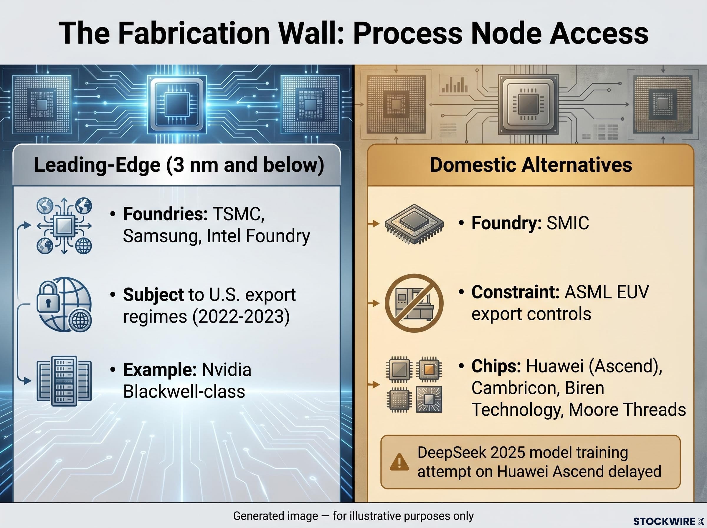
In 2025, DeepSeek attempted to train its next model on Huawei’s Ascend processors, reportedly encouraged by Chinese authorities. The attempt failed to meet expectations and delayed the model’s release, illustrating how far domestic chips still lag for critical AI workloads.
Being one or more nodes behind is not a minor handicap. It compounds through larger die area for equivalent logic, higher power consumption, and worse cost per unit of compute. For you, this is the section that explains why the chip problem cannot be solved by simply spending more money. The fabrication constraint is externally imposed and directly limits what physics can achieve regardless of engineering talent or capital.
| Chip programme | Accessible process node tier | Primary fabrication source | Benchmark positioning (approximate) |
|---|---|---|---|
| Nvidia Blackwell-class | Leading-edge (3 nm and below) | TSMC | Global performance leader |
| Huawei Ascend (current generation) | One or more generations behind frontier | SMIC (DUV-based) | Below Nvidia on standard AI benchmarks |
| Hypothetical DeepSeek first-generation chip | Constrained to domestically accessible nodes | SMIC or equivalent domestic foundry | Expected to trail both Nvidia and hyperscaler silicon on broad benchmarks |
Process nodes attract the headlines, but a second constraint may be equally decisive for inference performance, and it receives far less attention.
Large language model inference is frequently memory-bandwidth bound. That means the chip spends more time waiting to move model weights and activations between memory and compute units than it spends performing arithmetic. High-bandwidth memory, or HBM, solves this by stacking DRAM chips close to the processor die and using very wide data interfaces to deliver the throughput that inference workloads demand.
HBM supply is dominated by three manufacturers: SK Hynix, Samsung, and Micron. All three face U.S. trade measures that restrict advanced HBM shipments to Chinese entities. Chinese domestic efforts to develop HBM-equivalent solutions exist but lag in both performance and manufacturing capability, facing their own equipment and materials constraints.
HBM supply constraints extend well beyond DeepSeek’s situation: SK Hynix projects a global DRAM shortage lasting through 2030, with industry-wide HBM inventory sitting at just 3-4 weeks and all three major producers fully sold out through 2026, meaning that even well-capitalised buyers without export control exposure face meaningful allocation risk.
Without advanced HBM, a chip designer has several architectural strategies to reduce memory bandwidth dependence, each with trade-offs:
DeepSeek’s existing efficiency techniques are useful here. The company has already demonstrated that software and architectural tricks can reduce bandwidth pressure at the margins. But these approaches operate within limits. They cannot substitute for the raw throughput advantage that HBM provides at scale. A well-designed inference engine using deterministic execution patterns (as Groq has demonstrated) can partially work around bandwidth constraints, but even such architectures benefit enormously from high-bandwidth memory when available.
Even if a DeepSeek chip achieves strong compute density on restricted nodes, the HBM constraint can cap real-world inference throughput at a level that makes it uncompetitive for large model serving. This is a second independent ceiling on performance, separate from the fabrication node gap, and it means the barriers compound rather than simply add.
The target is not fixed. Any DeepSeek chip released in the next several years would compete not against today’s hardware, but against whatever Nvidia, the hyperscalers, and domestic Chinese players have shipped by then. The gap must be closed on a moving track, not a stationary one.
Three competitive tiers define the field:
The inference accelerator market is projected to represent approximately 80% of AI accelerator demand by 2030, which means the competitive tier a DeepSeek chip would enter is being reshaped simultaneously by Nvidia’s own inference investments and by the hyperscaler custom silicon programmes that are most competitive precisely in the inference segment.
Nvidia’s CUDA ecosystem has been in development for approximately 19 years as of mid-2026. That is not a feature list. It is a moat built in developer hours, framework integrations, and switching costs that no new chip can replicate on a short timeline.
The competitive challenge is not about matching a specific benchmark today. It is about competing against the next generation of all three tiers simultaneously, each of which is investing billions to extend its lead.
Based on industry experience and the constraints above, a credible first-generation inference chip from DeepSeek is realistically a 3-5 year project from serious initiation, assuming the company can hire experienced silicon engineers and sustain multimillion-dollar annual investment. That chip will almost certainly not match Nvidia’s leading-edge GPUs or hyperscaler internal accelerators on broad benchmarks.
But matching them is not the right success criterion. The realistic and strategically meaningful definition of success is narrower: a domestically manufacturable inference chip that runs DeepSeek’s own models at competitive cost per inference in Chinese datacenters, without depending on restricted foreign hardware. That is a supply chain de-risking achievement, not a benchmark crown.
Three paths could close the full performance gap with leading global AI silicon, each with different feasibility under current conditions:
DeepSeek is a bellwether. Its training efficiency, roughly one-tenth the cost of comparable U.S. frontier models, already demonstrated that algorithmic ingenuity can partially offset hardware disadvantages. That finding cuts in two directions simultaneously: it validates export controls as having real bite (the hardware gap is genuine and costly to work around), and it illustrates why controls alone are unlikely to constitute a sufficient long-term strategy (determined actors find ways to innovate within constraints).
Whether China develops a robust, independent semiconductor ecosystem is a question that will be answered over a decade, not a single product cycle. DeepSeek’s chip programme is one of the clearest real-world tests of how much of the AI hardware gap can be closed through focused ingenuity under substantial geopolitical constraints. The answer matters for semiconductor supply chains, AI policy, and competitive dynamics far beyond one company’s product roadmap.
The barriers facing DeepSeek fall into three categories, each independently difficult and together compounding: multi-year technical engineering timelines, fabrication and memory supply chain constraints imposed by export controls, and a competitive field that is moving forward at pace. The software challenge DeepSeek has already cleared operates on fundamentally different cost and time curves from the hardware challenge ahead.
What DeepSeek genuinely brings to the problem is real: proven hardware-software co-optimisation thinking, focused workloads it understands intimately, and a strategic necessity that concentrates effort in ways that broad-market chip companies cannot match. These are the same ingredients that have produced effective niche accelerators elsewhere.
The $5.6 million training cost that rattled markets was an algorithmic achievement. It does not transfer to fabrication economics. The 3-5 year timeline for a credible first-generation inference chip reflects a different kind of problem entirely.
For investors drawing portfolio conclusions from the DeepSeek training cost story, our deep-dive into AI ecosystem switching costs examines why the hardware versus software framing obscures the variable that actually drives long-term returns: ecosystem ownership and the re-platforming costs embedded in developer workflows.
The question worth carrying forward is not whether DeepSeek will build an Nvidia killer. It is whether the company can build a chip that is good enough to make its own inference operations sovereign and sustainable. That narrower question remains genuinely open.
This article is for informational purposes only and should not be considered financial advice. Investors should conduct their own research and consult with financial professionals before making investment decisions. Forward-looking statements regarding chip development timelines, competitive dynamics, and policy trajectories are speculative and subject to change based on technological developments, market conditions, and regulatory decisions.
Building an AI chip requires five distinct phases: architecture and logic design, verification and physical design, fabrication and packaging, bring-up and tooling, and ecosystem integration. Industry experience from Google, Amazon, and multiple AI chip startups points to a typical timeline of 3-5 years from serious project initiation to reliable high-volume production.
The $5.6 million training cost reflects algorithmic efficiency in software, a discipline that compresses very differently from hardware. Mask sets, foundry tape-outs, and chip verification do not compress the way training budgets do, and fabrication access is blocked by U.S. export controls regardless of available capital.
U.S. export controls, maintained since 2022-2023, use performance-threshold and whitelist mechanisms that bar Chinese AI firms from accessing leading-edge foundries like TSMC and Samsung for high-performance parts. They also restrict advanced HBM memory shipments from SK Hynix, Samsung, and Micron to Chinese entities, creating a compounding constraint on both fabrication and memory.
Large language model inference is frequently memory-bandwidth bound, meaning the chip spends more time moving model weights between memory and compute units than performing arithmetic. High-bandwidth memory (HBM) solves this problem, but advanced HBM supply is dominated by SK Hynix, Samsung, and Micron, all of which face U.S. trade measures restricting shipments to Chinese entities.
A credible first-generation DeepSeek inference chip would almost certainly not match Nvidia or hyperscaler silicon on broad benchmarks. The strategically meaningful success criterion is narrower: a domestically manufacturable chip that runs DeepSeek's own models at competitive cost per inference in Chinese datacenters without depending on restricted foreign hardware.