
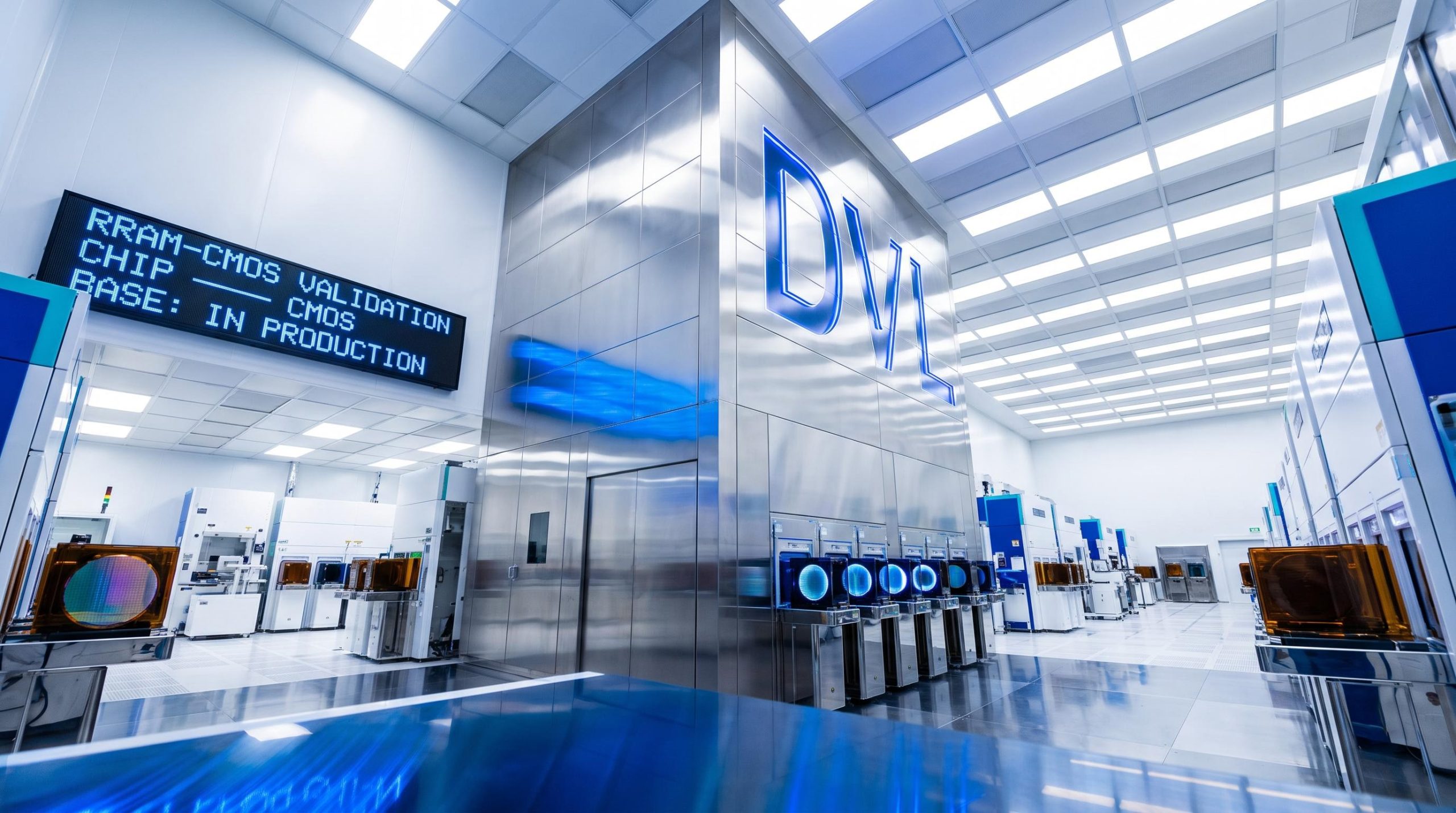
Silicon fabrication begins on dorsaVi’s first RRAM-CMOS validation chip
dorsaVi Limited (ASX: DVL) has commenced silicon manufacturing of its first RRAM-CMOS validation chip, with wafer processing now underway at the semiconductor foundry. The milestone follows the recently announced commencement of tape-out and marks the point at which the validation chip moves from design and data preparation into physical silicon production.
The step advances dorsaVi’s RRAM programme from concept toward a testable, physical product targeting the Physical AI memory market. Management sees the platform as critical memory infrastructure across exoskeletons, robotics, autonomous systems and IoT edge sensors.
Key highlights:
-
Manufacturing data package accepted into the foundry fabrication flow
-
CMOS base now in production, with the front-end wafer run underway
-
Programme progressed from design submission to an active wafer run
-
Builds toward the RRAM platform as memory infrastructure for the Physical AI market
When big ASX news breaks, our subscribers know first
What has actually commenced in the fab
Wafer processing starting means the physical silicon for the validation chip is now being produced, following successful passage through the foundry intake process. Foundry acceptance confirms the design met the foundry’s manufacturability requirements and that a wafer lot has been committed to the fabrication flow.
The current run is producing the front-end CMOS base, which includes the transistor and circuit-level structures that will later support the RRAM memory array, peripheral circuits and evaluation features. The RRAM-specific steps follow front-end processing.
The staged pathway ahead is expected to progress through the following:
-
Front-end CMOS wafer processing (current stage)
-
Wafer release for partner-led integration
-
BEOL (back-end-of-line) preparation
-
RRAM stack integration
-
Electrical characterisation and benchmarking
Educational: What is RRAM and why does memory matter for Physical AI?
RRAM is a non-volatile memory technology. Its appeal lies in bringing memory and compute closer together, reducing the latency and energy consumed when moving data between memory and processing circuits.
“Physical AI” refers to intelligence moving out of the cloud and onto the device itself, where systems must sense, decide and act in real time. As this shift accelerates, memory increasingly becomes the binding constraint. dorsaVi describes its platform as “critical memory infrastructure” and is positioning to supply that critical memory layer as a “licensable memory layer” for the wider Physical AI market.
For investors, the significance is directional. As intelligence migrates on-device, the company aims to occupy a foundational layer in the hardware stack that these systems depend on.
The neuromorphic robotics platform validation projected performance gains of up to 10x by bringing memory, signal conversion, and selected compute functions closer together, targeting markets including the global exoskeleton segment projected to reach US$1.79 billion by 2033 and humanoid robotics projected at US$38 billion by 2035.
Why the milestone matters for investors
Commencement of manufacturing carries value primarily through de-risking. Passing foundry acceptance removes an early technical hurdle, building the CMOS base creates the foundation for RRAM integration, and each staged step moves the programme closer to silicon-level testing.
| Milestone Achieved | What It Confirms | Investor Significance |
|---|---|---|
| Foundry acceptance | Design met manufacturability requirements | Removes key early-stage technical risk |
| CMOS base in production | Foundation layer for RRAM integration being built | Enables the next integration step |
| Staged execution pathway | Each step de-risks the programme | Moves closer to silicon-level testing |
Commercial opportunity across the Physical AI market
Manufacturing converts the RRAM programme from a design into physical silicon that can be tested and shown to partners and customers. It establishes the CMOS foundation for dorsaVi’s future products, targeting the markets where local, low-power memory is described as the binding constraint.
The target markets include:
-
Smart exoskeletons and EMG sensor nodes
-
Robotic joint controllers
-
Drones and autonomous vehicles
-
Always-on IoT edge sensors
The company sees a pathway from internal use toward a licensable component for the wider Physical AI hardware market. Each completed stage also removes technical and execution risk that a commercial partner weighs before committing, which management states supports future supply, partnering and licensing discussions.
CEO commentary
Mathew Regan, Group Chief Executive Officer, dorsaVi
“Physical AI is moving intelligence out of the cloud and into the device, where systems must sense, decide and act in real time. A critical constraint on that shift is the latency and energy consumed moving data between memory and processing. Our 22-nm RRAM Program with NTU and ITRI is designed to address that constraint by bringing memory and compute closer together. The current 180-nm validation run is a key stage within that broader program. Commencement of CMOS wafer fabrication moves our first RRAM-CMOS validation chip from completed design into physical implementation and is intended to generate the silicon-level learning required to inform and de-risk our subsequent 22-nm implementation. The speed, energy efficiency, endurance and non-volatility targeted by the program are the characteristics required by robot joints, exoskeleton nodes and intelligent sensors to make decisions locally rather than sending data to the cloud and waiting for a response. We intend to prove this memory architecture through our own sensing platform and then, subject to successful validation, commercialise it for the wider Physical AI market.”
Current program status and next steps
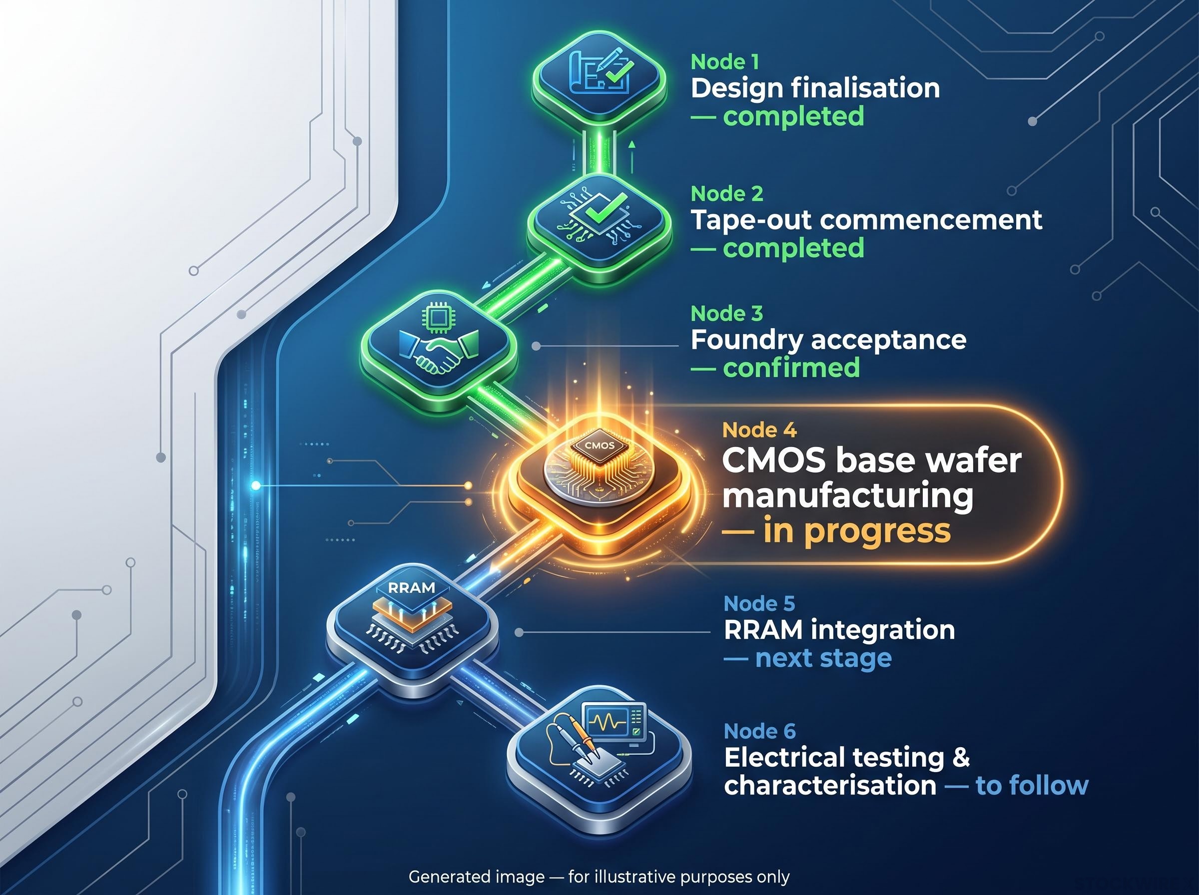
The programme has now cleared several defined stages, with wafer manufacturing of the CMOS base in progress and RRAM integration set to follow.
-
Design finalisation — completed
-
Tape-out commencement — completed
-
Foundry acceptance — confirmed
-
CMOS base wafer manufacturing — in progress
-
RRAM integration — next stage
-
Electrical testing & characterisation — to follow
Manufacturing converts the RRAM programme from design into physical silicon that can be tested and shown to partners, strengthening dorsaVi’s position toward commercialisation. Subject to successful validation, the company intends to prove the architecture through its own sensing platform before pursuing broader commercial opportunities across the Physical AI market.
Investors exploring the longer-horizon architecture context should review our deep-dive into the 22nm development program, which covers the performance targets at the advanced node, including write voltages below 2.0V, retention above 10 years at 125°C, and compute-in-memory efficiency exceeding 20 TOPS/W, alongside the industry data on AI memory bottleneck economics.
Don’t Miss the Next Tech Breakthrough Before the Market Moves
Get FREE breaking ASX tech news delivered to your inbox within minutes of release, complete with in-depth analysis. Join 20,000+ subscribers already ahead of the market on emerging opportunities. Click the “Free Alerts” button at StockWire X to start receiving alerts the moment market-moving announcements drop.