dorsaVi Finalises First RRAM Chip Design and Moves to Silicon Fabrication

dorsaVi has finalised the full design package for its first integrated RRAM-CMOS validation chip, developed in conjunction with NTU Singapore and ITRI Taiwan. The design is now ready for tape-out and staged silicon implementation, transitioning the program from design phase to physical fabrication.
dorsaVi completes RRAM-CMOS chip design, moves to fabrication
The completed design incorporates three validated capabilities: self-checking write-and-verify circuitry, compute-in-memory operation, and BEOL integration on commercial CMOS. The chip uses commercial CMOS front-end wafers sourced through TSMC, followed by partner-led BEOL and RRAM integration.
This milestone represents a concrete de-risking step for investors tracking technical execution, moving the program from theoretical design into physical silicon validation under standard commercial foundry conditions.
When big ASX news breaks, our subscribers know first
What is RRAM and why does it matter for edge computing?
RRAM (Resistive Random Access Memory) stores data through resistance states rather than charge storage. In conventional architectures, data must shuttle repeatedly between separate memory and processor units, creating bottlenecks in power consumption and response time. Ultra-edge intelligence refers to AI-driven decisions made locally at the point of sensing, without cloud connectivity.
dorsaVi’s existing wearable sensor technology provides the application layer for this capability, capturing and quantifying human movement data in real-time situations for up to 24 hours. RRAM technology is designed to enable on-device intelligence within this sensor platform.
RRAM offers three key characteristics for edge computing:
- Non-volatile storage: Retains data without power, allowing devices to wake up calibrated without reload cycles
- Combined storage and compute: Can perform calculations directly within the same array that stores data
- BEOL integration: Sits above standard CMOS transistor layers without altering foundry processes
Write-and-verify circuitry targets memory reliability
RRAM resistance states can vary due to device-to-device variation, cycle-to-cycle variation, array parasitics, and operating conditions. If a programmed cell sits too close to the sensing threshold, the read circuit may have reduced margin when distinguishing between stored “1” and stored “0” states.
The implemented write-and-verify circuitry addresses this by reading back the programmed RRAM state after each write operation and checking whether it falls within the intended resistance window. If the state is marginal or outside the target window, the circuit can support further tuning or re-programming.
The circuitry provides four verification functions:
- Post-write state verification before data is treated as successfully programmed
- Controlled re-programming path for states outside the target window
- Improved sensing margin through reduced marginal cell count
- Reliability and yield learning data for future algorithm optimisation
Reliable local memory operation is essential for target applications in defence, medical devices, exoskeletons, robotics, and industrial AI where failure tolerance is minimal. The write-and-verify function provides practical silicon data on programming behaviour across the array, supporting future optimisation of sensing schemes, array yield, and long-term memory reliability.
Thermal stability validation against AEC-Q100 automotive-grade methodology confirmed fully reversible cell behaviour at temperatures up to 150°C, a result that directly supports the reliability requirements of sealed industrial enclosures and high-heat robotics deployments targeted by the platform.
Compute-in-memory reduces power and latency
In conventional architectures, repeatedly moving data between memory and a separate processor is a major source of power consumption and latency in edge devices operating under tight energy and response-time constraints. dorsaVi’s design addresses this by allowing selected compute operations to occur closer to where the data is stored.
The chip includes purpose-built Compute-in-Memory structures that operate in two modes: binary memory mode for conventional data storage and retrieval, and compute-in-memory mode that uses programmed resistance states as compute weights. In CIM mode, the array accumulates across up to 64 inputs locally before producing a compact digital compute output through the CIM readout path.
| Mode | Function | Benefit |
|---|---|---|
| Binary Memory Mode | Stores and retrieves digital data conventionally | Standard memory operation |
| Compute-in-Memory Mode | Uses resistance states as compute weights, accumulates locally | Reduces data movement, lowers power, faster local decisions |
This validates how future RRAM-based hardware may enable on-device AI without cloud round-trips, addressing critical requirements for latency-sensitive and power-constrained edge applications.
BEOL integration provides scalable manufacturing pathway
Commercial CMOS foundation
Rather than requiring changes to the CMOS transistor layer, dorsaVi’s RRAM integration is designed around the chip’s back-end-of-line (BEOL) metal layers, which sit above the standard CMOS front-end transistor circuitry. This means the validation chip uses commercial CMOS front-end wafers sourced through TSMC, followed by partner-led BEOL and RRAM integration steps, with no changes required to the CMOS transistor layer.
The BEOL integration approach provides four manufacturing advantages:
- Commercial CMOS foundation without redesigning the underlying transistor platform
- BEOL-compatible integration preserves front-end device structure during memory layer addition
- Future density scaling potential in upper integration layers supports more compact memory-compute architectures
- Scalable manufacturing pathway for process optimisation and node migration
This integration approach de-risks manufacturing scalability by building on established foundry processes rather than requiring custom fabrication lines. The program is designed to generate practical silicon data needed to support future process optimisation, manufacturability assessment, and potential migration to more advanced technology nodes.
Target markets span exoskeletons, defence, robotics, and industrial AI
Smart exoskeletons represent the lead market for this technology. Smart EMG sensor nodes read muscle signals to determine user intent (swing, push-off, fatigue) and send commands instead of streaming raw data. The application requires fast writes inside the control loop and non-volatile storage for each user’s baseline profile.
Secondary markets include robotics, where joint controllers run individual position and torque loops and hold calibration data. Fast mid-loop updates and non-volatile memory that survives power cycles allow robotic limbs to wake up calibrated without re-homing sequences. On-device industrial AI applications require model weights held non-volatile and positioned next to compute resources.
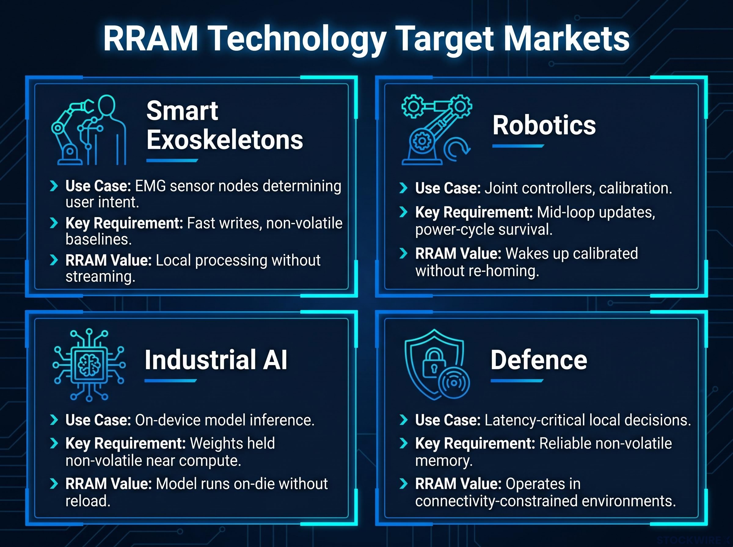
| Sector | Use Case | Key Requirement | RRAM Value |
|---|---|---|---|
| Smart Exoskeletons | EMG sensor nodes determining user intent | Fast writes, non-volatile baselines | Local processing without streaming |
| Robotics | Joint controllers, calibration | Mid-loop updates, power-cycle survival | Wakes up calibrated without re-homing |
| Industrial AI | On-device model inference | Weights held non-volatile near compute | Model runs on-die without reload |
| Defence | Latency-critical local decisions | Reliable non-volatile memory | Operates in connectivity-constrained environments |
These sectors represent high-value applications where local, low-power, non-volatile intelligence is a competitive necessity rather than an incremental improvement. The technology addresses requirements for real-time decision-making without cloud connectivity across industrial, clinical, and autonomous systems applications.
Next steps and commercialisation pathway
With the design package finalised, the chip proceeds to tape-out as scheduled. Validated silicon will progress toward embedding directly into dorsaVi’s wearable sensor hardware, enabling on-device intelligence without external processing.
The company will engage with prospective partners and customers across exoskeleton, defence, robotics, and industrial AI markets to evaluate fit and progress toward commercial deployment. Results are expected to inform the Company’s subsequent 22-nm implementation pathway.
For investors wanting to understand the performance targets underpinning this roadmap, our deep-dive into the 22nm RRAM development program covers the write voltage, retention, and compute-in-memory efficiency benchmarks the program is designed to achieve at the commercially relevant advanced node.
The program advances on three fronts:
- Tape-out proceeds as scheduled for physical fabrication
- Integration into dorsaVi’s wearable sensor platform for on-device intelligence deployment
- Market evaluation and commercialisation engagement with target sectors
The next major ASX story will hit our subscribers first
CEO frames milestone as path to commercial scale
Mathew Regan, Group Chief Executive Officer
“Finalising the design of our first RRAM-CMOS validation chip is a significant milestone for the program. It confirms the architecture is manufacturable under standard commercial foundry conditions and clears the path to the physical silicon we need to validate performance. We are now focused on fabrication and on using the results to advance the program toward commercial scale.”
Management commentary emphasises execution focus and commercial intent rather than extended R&D timelines. The transition from design completion to fabrication represents a concrete step toward validating the architecture’s performance under commercial foundry conditions.
Want the Next MedTech Breakthrough in Your Inbox?
Join 20,000+ investors receiving FREE breaking ASX news within minutes of release, complete with expert analysis. Click the “Free Alerts” button at Big News Blast to get real-time alerts on market-moving MedTech developments before the crowd reacts.