Why JPMorgan’s 2026 Sector Calls Split Banks and Energy Apart
1 hr ago

Bank of America’s NT$2,560 price target on TSMC rests on a specific empirical claim: that Samsung and Intel’s competing nodes are each running at an estimated 20,000-25,000 wafers per month, against TSMC’s trajectory toward approximately 180,000 wafers per month at 3nm by end-2026 alone. That capacity gap is not a forecast. It is the current state of the competitive field.
With AI infrastructure spending accelerating across hyperscalers and TSMC’s HPC segment now representing approximately 61% of total revenue, the question for investors is not whether demand is real but whether a credible competitive threat exists that could erode pricing power or customer concentration over a 12-24 month horizon. BofA’s reaffirmed Buy rating, issued following TSMC’s Taiwan technology symposium in May 2026, argues directly that the threat is overstated. What follows examines why, using the specific technical and capacity metrics that underpin that conclusion, and equips investors with a framework for interpreting yield rates, wafer capacity figures, node timelines, and advanced packaging data as signals of competitive moat.
The TSMC Q1 2026 earnings report confirms that HPC accounted for 61% of net revenue that quarter, with advanced technologies at 7nm and below contributing 74% of total wafer revenue, and capital appropriations of US$31.3 billion committed to advanced technology capacity and fab construction.
The numbers first.
TSMC is projected to reach approximately 180,000 wafers per month at 3nm by end-2026, rising to 230,000 by 2027. Samsung SF3 and Intel 18A are each estimated at 20,000-25,000 wafers per month.
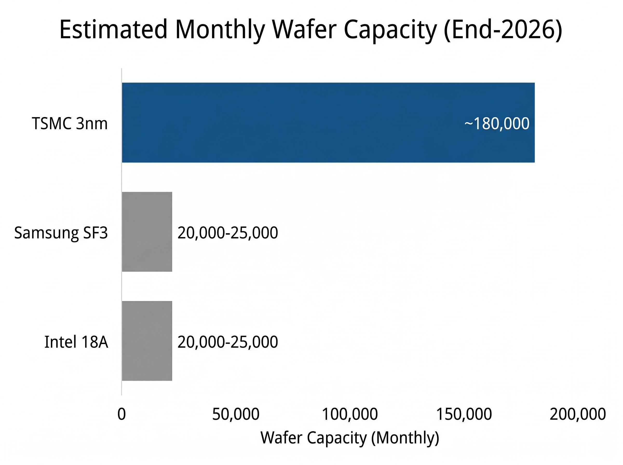
That is not a percentage lead. It is an order-of-magnitude difference in revenue-generating capacity at the nodes where AI accelerators, flagship mobile processors, and high-performance computing chips are manufactured.
Wafers per month measures something more concrete than transistor density claims or process generation naming conventions. It captures how many chips a foundry can actually produce and ship to paying customers in a given period. A node that exists in engineering samples but runs at 25,000 wafers per month generates a fraction of the revenue, ecosystem lock-in, and manufacturing learning of one running at nearly eight times that volume.
TSMC’s 3nm capacity is not merely large; it is fully utilised. Apple, Nvidia, AMD, and Qualcomm are locked into the node through 2026 and beyond, making customer displacement structurally difficult in the near term. The company targets 25% compound annual capacity growth for 3nm and 5nm nodes from 2022 to 2027.
| Node | Producer | Est. Monthly Wafer Capacity (2026) | Key External Customers | Utilisation Status |
|---|---|---|---|---|
| N3 (3nm) | TSMC | ~180,000 | Apple, Nvidia, AMD, Qualcomm | Fully utilised |
| SF3 (3nm-class) | Samsung | ~20,000-25,000 (est.) | Internal / existing customers | Limited external adoption |
| 18A | Intel | ~20,000-25,000 (est.) | No major named wins at scale | Ramping; yields improving |
Capacity utilisation at leading-edge nodes is a direct proxy for pricing power and customer stickiness. An investor evaluating TSMC’s durability against competitive narratives starts here, not with transistor counts.
Yield rate is the percentage of usable chips produced from each silicon wafer. A low yield means most chips come off the line defective; a high yield means the manufacturing process is mature enough to produce revenue-generating output consistently. Yield improves over time as engineers identify and eliminate defect sources, which is why it serves as a lagging but high-conviction signal of process maturity and cost structure.
Three steps connect yield data to a competitive reading:
Samsung foundry yield constraints at 3nm, estimated at approximately 55-60% compared to TSMC’s mature process yields, represent the clearest reason why Apple’s early-stage diversification talks have not translated into confirmed volume orders, and why any realistic capacity shift remains capped well below 10% of Apple’s total chip demand before 2027.
TSMC is deploying five fabrication facilities simultaneously at N2 while reducing technology transfer durations by approximately 20%, compressing the time between process development and full-scale production.
The gap between a process announcement and an external customer win at volume is a more meaningful metric than the announcement itself. A node that exists in a roadmap presentation but has not attracted a named tier-1 customer at scale is not yet competing in the market that matters to investors.
As of mid-May 2026, no major AI GPU or accelerator volumes have been publicly confirmed for Samsung SF3 or Intel 18A at a scale comparable to TSMC N3 or N2. That absence is the competitive clock investors should be reading.
The competitive assessment most investors apply to TSMC focuses on logic nodes: who has the smallest transistors, the densest chips, the most advanced process generation. That assessment misses a separate, increasingly important axis of differentiation.
CoWoS (Chip-on-Wafer-on-Substrate) and SoIC (System-on-Integrated-Chips) are advanced packaging technologies that connect multiple chiplets into a single package. They are distinct from the logic manufacturing process itself. In AI chip design, where Nvidia’s H100, H200, and B100 series and AMD’s Instinct/MI-series products combine multiple silicon dies into a single unit, the packaging layer determines whether the final product can be assembled at scale with acceptable yield.
TSMC’s CoWoS yield exceeds 98%. Intel’s competing EMIB-T pilot yield currently sits at 80%-85%, with a 95% mass production yield target required by mid-2027.
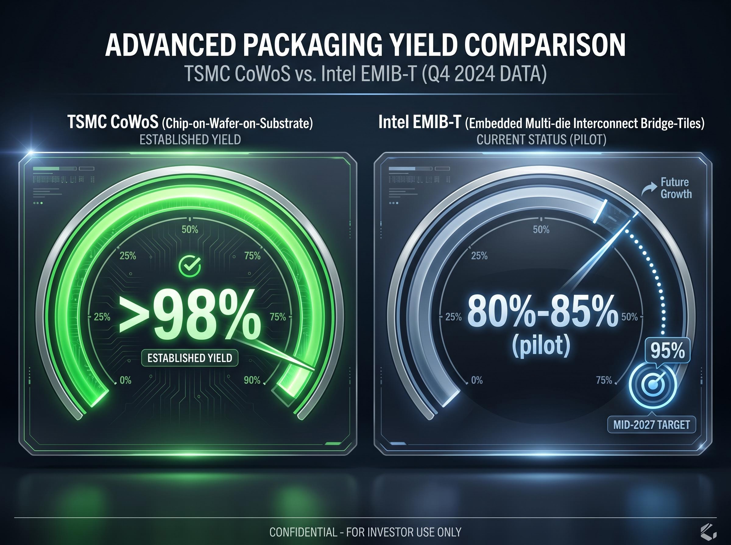
That gap sets a concrete, time-bounded competitive test. Mid-2027 is the milestone.
The TrendForce CoWoS versus EMIB analysis highlights that while EMIB carries a cost advantage over CoWoS, the yield differential between the two technologies remains the primary gating factor for hyperscaler adoption decisions, reinforcing why the mid-2027 mass production yield milestone for EMIB-T functions as a concrete competitive test rather than a speculative timeline.
| Packaging Technology | Producer | Current Yield | Mass Production Target | Growth Rate (CAGR to 2027) |
|---|---|---|---|---|
| CoWoS | TSMC | >98% | At scale (fully booked) | ~80% |
| SoIC | TSMC | Not publicly disclosed | Ramping | ~90% |
| EMIB-T | Intel | 80%-85% (pilot) | 95% by mid-2027 | Not disclosed |
CoWoS capacity is described as fully booked and a bottleneck for AI GPU shipments through end-2025 and beyond. Nvidia, AMD, and hyperscaler custom ASICs all depend on TSMC’s interposer-based packaging. The yield gap between CoWoS and EMIB-T gives investors a verifiable milestone to monitor as a signal of whether competitive parity is approaching.
TSMC’s concentration in Taiwan has historically weighed on the company’s valuation multiple relative to its earnings power. Investors apply a probability-weighted discount for geopolitical scenarios that could disrupt production. The overseas fab expansion addresses that discount directly.
Geopolitical supply chain fragmentation has accelerated the conditions under which TSMC’s overseas fab expansion carries valuation significance, as competing national industrial policies from the US, EU, and China are simultaneously incentivising domestic semiconductor capacity through export controls and subsidy regimes that structurally favour foundries with multi-geography production footprints.
The Arizona (USA) and Kumamoto (Japan) facilities ramping through 2025-2026 serve three distinct functions:
The valuation case for overseas fabs is primarily about reducing the geopolitical discount, not about near-term wafer output. Analyst consensus positions overseas capacity as a de-risking tailwind supporting multiple expansion.
TSM ADR was trading in the $404-$411 range as of mid-May 2026, against a 12-month consensus price target averaging approximately $463-$466. BofA’s NT$2,560 target sits above the consensus average of approximately NT$2,490-2,515. The gap between the current price and these targets reflects, in part, the degree to which the market has or has not priced in the de-risking effect.
Analyst consensus (MarketBeat): 2 Strong Buy, 11 Buy, 2 Hold, 0 Sell.
BofA’s NT$2,560 target sits above the consensus average. The question is what specific analytical premises justify that premium.
The answer maps directly to the technical evidence examined in the preceding sections. BofA’s above-consensus positioning reflects conviction on three fronts: that TSMC’s yield leadership at N2 and N3 is widening rather than narrowing, that the capacity scale advantage at approximately 180,000 wafers per month (3nm) versus 20,000-25,000 at competing nodes is durable through 2027, and that the advanced packaging moat (CoWoS at >98% yield) compounds the logic node advantage in ways that consensus models may underweight.
TWSE-listed shares last closed at approximately NT$2,265 as of mid-May 2026, implying approximately 10-11% upside to consensus and greater upside to BofA’s target. TSMC’s N2 capacity targets a 70% CAGR from 2026-2028, providing the growth trajectory that supports the premium valuation.
A price target only has value if investors understand the conditions required for it to hold. Three monitoring milestones warrant tracking:
BofA’s core argument, restated in one sentence: TSMC’s combined advantage in leading-edge capacity scale, yield maturity, and advanced packaging creates a competitive moat that neither Samsung nor Intel can credibly challenge within a 12-24 month horizon.
A genuine competitive shift would require observable evidence that does not currently exist in publicly confirmed data as of mid-May 2026:
The Intel 18A revenue milestone of a first billion-dollar year in 2026 represents the threshold at which external customer interest in the node would begin translating into booking depth, but Intel’s stock fell approximately 3.85% on the day Apple’s preliminary talks became public, signalling that markets are pricing execution risk into the revenue trajectory rather than treating inbound customer interest as confirmed accretive volume.
The distinction that matters: marketing announcements, roadmap updates, and headline transistor density claims are not the metrics that signal competitive erosion. Customer wins at scale, yield parity in advanced packaging, and capacity absorption rates are.
This article is for informational purposes only and should not be considered financial advice. Investors should conduct their own research and consult with financial professionals before making investment decisions.
The technical and capacity evidence examined here points to a specific conclusion: BofA’s thesis is grounded in verifiable metrics that the broader consensus has not fully priced, rather than in generalised optimism about AI demand.
The three monitoring milestones identified above, Intel EMIB-T yield by mid-2027, named AI GPU customer wins at competing nodes, and TSMC N2 utilisation trajectory, provide the practical mechanism for updating that assessment over the next 12-24 months.
AI data centre operators account for approximately 70% of total memory shipments, signalling the structural depth of infrastructure investment that underpins TSMC demand. The AI buildout, quantified through hyperscaler capital expenditure trajectories and the depth of TSMC’s order book, provides a demand floor that positions competitive displacement as a medium-term consideration rather than a near-term threat.
Hyperscaler capital expenditure trajectories across Microsoft, Google, Amazon, and Meta represent a combined approximately $725 billion in 2026 guidance directed explicitly at agent-driven inference infrastructure, providing the demand floor that anchors TSMC’s order book depth and makes competitive displacement a medium-term rather than near-term consideration.
Investors evaluating semiconductor exposure should use the yield, capacity, and packaging metrics outlined here as a monitoring framework rather than treating analyst price targets as static signals.
Past performance does not guarantee future results. Financial projections are subject to market conditions and various risk factors.
Wafers per month measures how many chips a foundry can actually produce and ship to paying customers in a given period. It is a more concrete indicator of revenue-generating capacity than transistor density claims, making it a key metric for assessing TSMC's competitive moat versus Samsung and Intel.
CoWoS (Chip-on-Wafer-on-Substrate) is an advanced packaging technology that connects multiple chiplets into a single unit, used in AI chips like Nvidia's H100 and AMD's Instinct series. TSMC's CoWoS yield exceeds 98% compared to Intel's competing EMIB-T pilot yield of 80%-85%, meaning TSMC can assemble AI chips at scale with far fewer defects, reinforcing its position as the preferred supplier for hyperscalers.
As of mid-2026, Intel 18A entered high-volume manufacturing in late 2025 with yields described as adequate and improving, targeting industry-standard yield levels by 2027. By contrast, TSMC's N3 node is running at approximately 180,000 wafers per month, is fully utilised, and has locked-in customers including Apple, Nvidia, AMD, and Qualcomm through 2026 and beyond.
Three milestones are worth tracking: whether Intel's EMIB-T advanced packaging reaches 95% mass production yield by mid-2027, whether any tier-1 AI GPU customer publicly commits volume to Samsung SF3 or Intel 18A at scale, and whether TSMC's N2 node capacity remains sold out through 2027, confirming the demand floor that underpins analyst revenue assumptions.
The Arizona and Kumamoto facilities are primarily relevant as a geopolitical de-risking catalyst rather than a near-term production driver. Analysts expect overseas capacity to reduce the probability-weighted discount investors apply to Taiwan-specific risk scenarios, supporting multiple expansion even before the fabs reach full output.