Adisyn Clears Path to Tier 1 Chipmaker Talks With Repeatable Graphene Process
Adisyn achieves independent verification of graphene deposition below 300°C
Adisyn has achieved independent verification of repeatable graphene deposition technology that operates reliably below 300°C. Associate Professor Rakesh Joshi of UNSW Sydney’s Graphene Research Group confirmed the breakthrough following three independent experimental runs on separate days, each verified across 10 Raman Spectroscopy measurement spots.
The result clears Milestone 2 under the Share Sale and Purchase Agreement for the 2D Generation acquisition. Three UHR-TEM cross-sections confirm continuous graphene layer formation across the full 1×1 cm² coupon, demonstrating both repeatability across independent runs and uniformity across the coupon surface. This achievement transforms a laboratory result into a commercially credible process that semiconductor manufacturers can evaluate for integration.
Adisyn (ASX: AI1) now transitions from R&D proof-of-concept to active engagement with Tier 1 global semiconductor companies and process scale-up to wafer-level formats.
When big ASX news breaks, our subscribers know first
Why the 300°C threshold matters for semiconductor fabrication
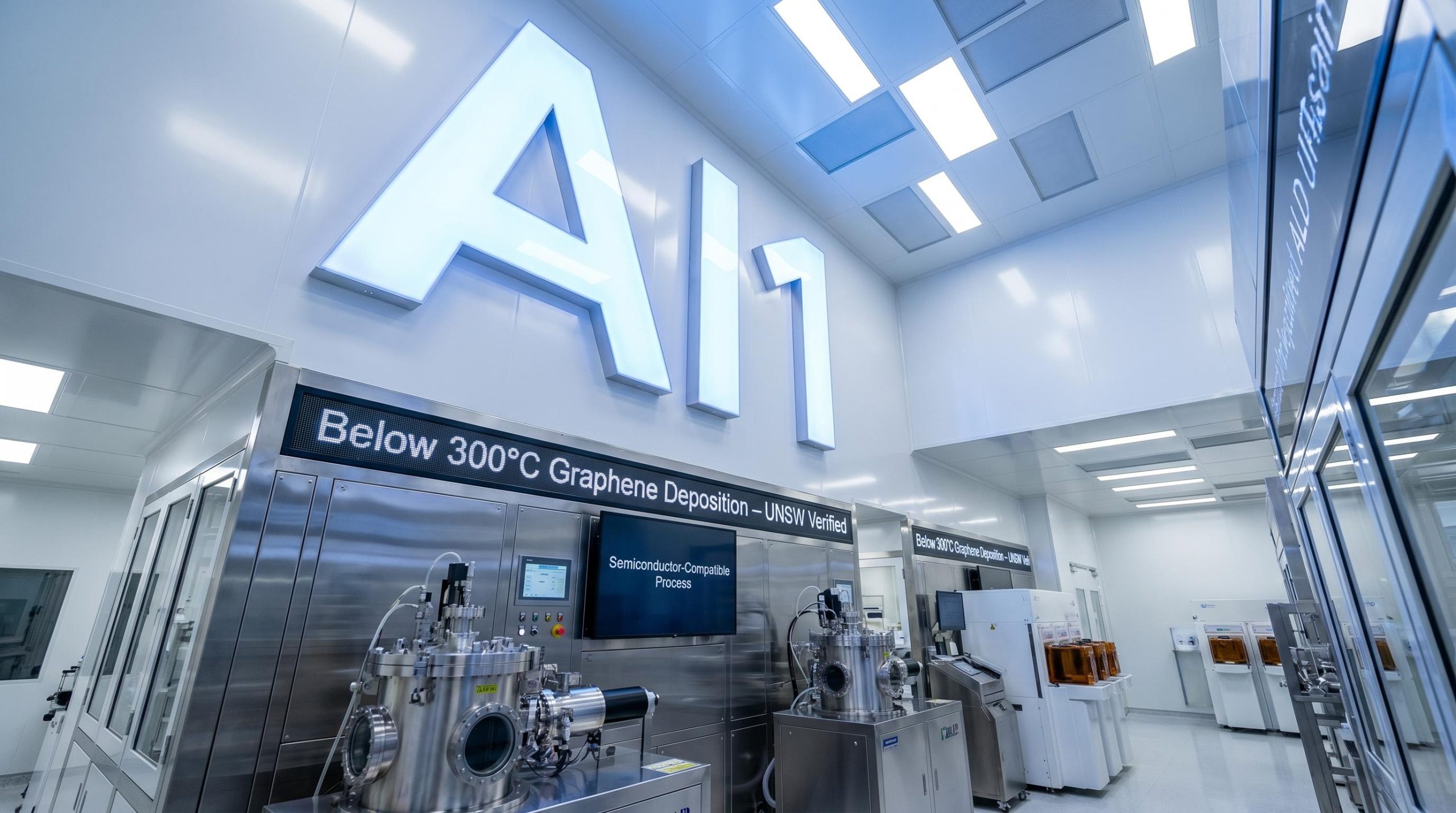
Semiconductor fabs impose strict thermal limits to protect existing chip structures during manufacturing. No previous graphene process deposited on an industrial scale deposition system has managed to reliably operate below this thermal limit. The wide process window temperature range demonstrated by Adisyn’s technology makes adoption by fabs significantly easier, as the process operates well below the industry’s critical thermal threshold.
The equipment choice removes another barrier to adoption. Atomic Layer Deposition is already a standard deposition method in leading-edge semiconductor fabs at TSMC, Samsung and Intel. A chipmaker evaluating Adisyn’s graphene process is anticipated to already have years of experience running ALD systems and will have detailed understanding of the requirements to implement the new technology.
This compatibility with existing fab equipment and thermal constraints shortens the path from validation to commercial integration. Breaking down these adoption barriers is critical to surpassing commercial thresholds.
Understanding graphene deposition and the copper interconnect challenge
Every advanced chip in AI servers, smartphones and data centres relies on copper interconnects — the microscopic wiring that links billions of transistors. As chips shrink below 2 nanometres, copper suffers increased electrical resistance. It generates excess heat, wastes power and limits signal speed.
The semiconductor industry has known for years that graphene, with its extraordinary electrical and thermal properties, is the logical successor material. The problem has been getting graphene to grow inside a chip fab using existing equipment without exceeding the temperature thresholds that would damage chip structures already in place.
Adisyn’s process addresses this structural challenge directly. The combination of industrial ALD equipment, semiconductor-compatible temperatures and confirmed repeatable film formation provides the foundation for commercial conversations that were previously not possible.
Technical verification confirms process consistency
The company demonstrated continuous graphene film formation on a copper substrate using an industrial Atomic Layer Deposition system with all process steps maintained below 300°C. The graphene layer, confirmed at approximately 1-2 nm thickness, was verified by two independent characterisation methods.
| Verification Method | What It Measured | Result |
|---|---|---|
| Raman Spectroscopy | Graphene spectral signatures | Consistent across 10 measurement spots per coupon |
| UHR-TEM Imaging | Cross-section layer structure | Continuous graphene layer, interlayer spacing 3.4 ± 0.3 Å |
UHR-TEM imaging was conducted at Hebrew University of Jerusalem. The cross-section electron microscopy confirmed a continuous graphene layer with interlayer spacing of 3.4 ± 0.3 Å, consistent with characteristic graphite structure, and lateral continuity across several micrometres.
The repeatability finding separates this from laboratory curiosity. Adisyn ran the same deposition recipe (YBPD-391) three times on separate days. Each run produced consistent graphene layer formation. The same layer structure appeared every time, confirmed across 10 Raman measurement spots per sample.
Critically, the layer was confirmed uniform across the coupon itself. Three separate cross-section samples taken from different positions across the same 1 cm² coupon produced identical results, demonstrating that the deposition process covers the substrate evenly, not just in isolated patches.
Independent expert credentials
Associate Professor Rakesh Joshi leads the Graphene Research Group at UNSW Sydney’s School of Materials Science and Engineering. His credentials establish the verification’s credibility for engagement with Tier 1 semiconductor companies:
- Theme Leader for Energy and Environment at the School of Materials Science and Engineering
- Chief Investigator in the ARC Centre of Excellence for Carbon Science and Innovation
- Over 130 peer-reviewed journal articles published
- Co-authored work with Nobel Laureate Sir Andre Geim at University of Manchester
- Five international patents
- Fellow of the Royal Society of Chemistry
Associate Professor Joshi was provided with the full Milestone 2 results dataset, comprising the three-run Raman repeatability data and UHR-TEM cross-section imaging, and has confirmed the results meet the Milestone 2 standard.
Milestone 2 triggers share consideration
Achievement of Milestone 2 results in the issue of 100 million fully paid ordinary shares to the original shareholders of 2D Generation. Additional shares will also be issued to eligible employees under the agreed incentive arrangements, reflecting their contribution to the delivery of Milestone 2.
Path to Milestone 3 and commercial engagement
The three-milestone structure under the Share Sale and Purchase Agreement establishes clear technical and commercial gates:
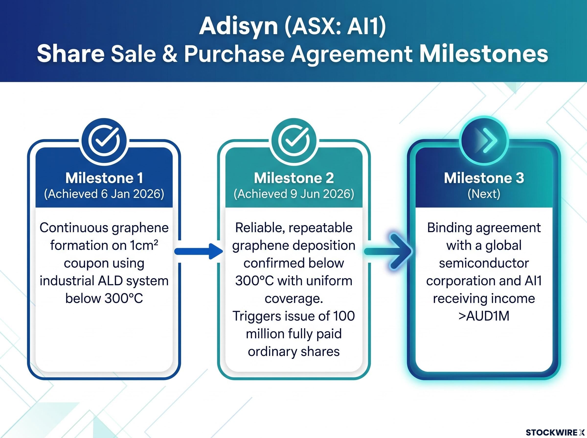
- Milestone 1 (achieved 6 January 2026): Demonstration of continuous graphene formation on 1cm² coupon using industrial ALD system below 300°C
- Milestone 2 (achieved 9 June 2026): Reliable, repeatable graphene deposition confirmed below 300°C with uniform coverage
- Milestone 3 (next): Binding agreement with a global semiconductor corporation and AI1 receiving income of more than AUD1M
With Milestone 2 independently confirmed, Adisyn moves into a new phase. The company will commence deeper engagement with Tier 1 global semiconductor manufacturers and fabrication facilities to explore collaboration, validation and integration pathways. In parallel, Adisyn will advance film quality optimisation and begin scale-up from 1×1 cm² coupon to full wafer-level substrates — the format required for commercial semiconductor manufacturing.
Arye Kohavi, Managing Director
“Achieving Milestone 2 with independent expert verification is a defining moment for Adisyn. Repeatability is what separates an interesting laboratory result from a process that the semiconductor industry can actually use. We have now demonstrated that our graphene deposition process works consistently, run after run, with uniform coverage across the coupon — and we have done so at temperatures that are fully compatible with existing chip fabrication environments.”
The next major ASX story will hit our subscribers first
Market context and investment thesis
The global semiconductor market is forecast to reach approximately US$1 trillion by 2030. Adisyn’s US patent grant, announced 7 May 2026, provides an IP protection foundation for commercial discussions.
The process deposits covalently bonded graphene at low temperatures without catalytic metal residues, and US patent protection covering the method, resulting products, and devices incorporating those products was granted by the USPTO in May 2026, reinforcing the IP foundation ahead of Tier 1 commercial discussions.
The investment case rests on demonstrated technical capability. Adisyn has now confirmed a repeatable, independently verified graphene deposition process that operates on standard fab equipment below semiconductor thermal limits. The combination of industrial ALD equipment compatibility, semiconductor-compatible temperatures, confirmed repeatable film formation and patent protection positions Adisyn to begin commercial conversations with Tier 1 manufacturers that were previously not possible.
Want the Next Tech Breakthrough in Your Inbox?
Join 20,000+ investors receiving FREE breaking ASX tech news within minutes of release, complete with in-depth analysis. Click the “Free Alerts” button at Big News Blast to get real-time alerts covering Healthcare, Finance, Consumer, Manufacturing and more the moment market-moving announcements hit the wire.