

EMASS holds its first 16nm chip
Nanoveu Limited (ASX: NVU) has announced a major technical milestone: engineering samples of its next-generation 16nm ECS-DoT edge AI system-on-chip (SoC) have been fabricated at Taiwan Semiconductor Manufacturing Company (TSMC) and delivered to EMASS, Nanoveu’s wholly owned semiconductor subsidiary.
The 16nm ECS-DoT program followed a clear sequence. Front-end design and physical design were completed with GDS sign-off in December 2025, tape-out followed in January 2026 when mask data was released to TSMC and wafer fabrication began, and packaged engineering samples have now been delivered to the EMASS engineering team.
This is the first time an ECS-DoT device has been produced at an advanced FinFET node. With physical silicon now in hand, bring-up, benchmarking and characterisation commence, and the company intends to publish a summary of measured results on completion.
When big ASX news breaks, our subscribers know first
What 16nm FinFET means for edge AI silicon
A process node refers to the size of the transistors etched onto a chip. In simple terms: the smaller the node, the more transistors fit on a die, and the less power they leak. Moving from 22nm to 16nm FinFET brings higher logic density, lower leakage current, and greater headroom for integrating more functionality on a single die.
For EMASS, this headroom is what enabled the 16nm ECS-DoT to carry a full Bluetooth Low Energy radio, a larger on-chip memory array, and additional accelerators on the same die, while remaining within the power budget the ECS-DoT family was designed around. The FinFET architecture achieves this through three-dimensional transistor structures that control current leakage more precisely than planar designs at equivalent or smaller dimensions.
This positions the 16nm ECS-DoT within an increasingly competitive edge AI silicon category, where integration density and power efficiency are among the primary design constraints.
What the 16nm chip carries
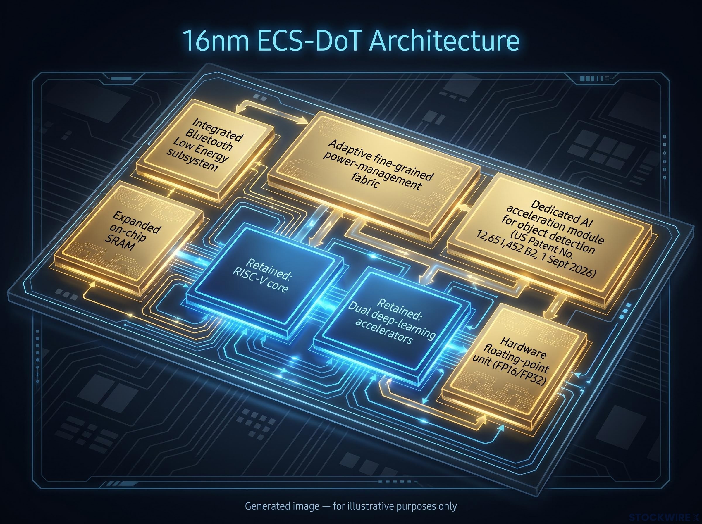
The 16nm ECS-DoT retains the RISC-V core, dual deep-learning accelerators, scalable compute-to-memory interconnect and always-on design philosophy of the 22nm generation, and adds or expands the following subsystems (as shown in gold in the block diagram, Figure 4, published in the announcement):
-
Integrated Bluetooth Low Energy subsystem: The full BLE signal chain, including the analog front end, RF transceiver, phase-locked loops and on-chip matching networks, is built into the SoC. In many designs this removes the need for a separate wireless component, reducing board area, bill-of-materials cost and design complexity for connected devices such as wearables, tags and industrial sensors.
-
Expanded on-chip SRAM: A substantial increase in on-chip memory supports larger neural networks and higher-throughput vision and multi-sensor workloads, and reduces the off-chip memory accesses that dominate energy consumption in many edge AI systems.
-
Adaptive fine-grained power-management fabric: EMASS’s most advanced power architecture to date, featuring fine-grained power gating across functional domains, dynamic clock gating and autonomous low-power states managed by internal controllers, delivering microsecond-level sleep and wake behaviour. The design achieves this without dynamic voltage and frequency scaling, relying instead on architectural and circuit-level techniques.
-
Dedicated AI acceleration module for object detection: A purpose-built engine for lightweight vision models including YOLO-Nano class networks, MobileNet-SSD detection heads and FOMO-style detectors. The non-maximum suppression stage of this module is the subject of US Patent No. 12,651,452 B2, exclusively licensed to EMASS, as announced on 1 September 2026.
-
Hardware floating-point unit: For the first time in the ECS-DoT family, the 16nm device includes an FPU supporting FP16 and FP32 operations, which speeds up digital signal processing and mixed-precision AI workloads and simplifies porting of existing floating-point code and libraries to the platform.
Full software and workflow compatibility with the 22nm ECS-DoT is maintained across all of the above.
| Feature | 22nm ECS-DoT | 16nm ECS-DoT | Investor Relevance |
|---|---|---|---|
| BLE connectivity | External component required | Integrated on-chip | BOM cost reduction; simpler board design for connected wearables and IoT |
| On-chip SRAM | Standard | Expanded | Larger AI models on-device; reduces off-chip power draw |
| Power management | Standard always-on | Fine-grained adaptive fabric | Longer battery life for wearables and asset tags |
| Object detection | Dual DL accelerators | Dedicated OD accelerator (patent protected) | IP moat; faster inference in vision applications |
| Floating-point unit | None | FP16/FP32 hardware FPU | Easier porting of existing AI libraries to the platform |
Two-node product family: a commercial structure, not just a roadmap
EMASS now holds ECS-DoT silicon at two process nodes simultaneously. The announcement describes this as the position an established semiconductor company works from: a commercial device winning design-ins while the next generation is characterised behind it. This is the first time EMASS has held both at once.
The 22nm ECS-DoT is the company’s commercial product, available for customer evaluation and design-in today. It is in customer evaluation and design-in across wearables, industrial sensing, asset tracking and smart infrastructure applications, including the asset-tracking reference design with Bosch Sensortec announced in July 2026.
Concurrent AI model execution on ECS-DoT silicon was demonstrated ahead of the 16nm delivery, with keyword detection and voice recognition running simultaneously on the 22nm device at 400-500 µW average power, establishing the always-on architecture’s multi-model capability before the expanded memory and FPU of the 16nm generation became available.
The Bosch Sensortec asset-tracking reference design, announced in July 2026, is among the active commercial evaluation platforms built on the 22nm ECS-DoT, combining five Bosch MEMS sensors with ECS-DoT edge AI inference for logistics, cold-chain and industrial IoT applications.
The 16nm ECS-DoT is the more fully integrated member of the family, aimed at customers who require more on-chip memory, who want to run vision alongside audio and sensor workloads, or who prefer the Bluetooth radio integrated within the SoC rather than as a separate board component. Critically, both devices share one programming model, software stack and toolchain. A customer can begin development on the 22nm today and migrate to the 16nm with minimal changes to application code, and EMASS can support both from a single engineering base.
Smaller process nodes remain on the roadmap for future ECS-DoT generations.
Dr Mohamed Sabry, Director of Nanoveu and Founder of EMASS
“There is a particular moment in every chip program when the first parts come back from the fab and you can hold what was, until then, a set of files. We have reached that moment with the 16nm ECS-DoT. It carries everything we set out to build: the radio, the memory, the power fabric, the detection engine and the FPU, on one die at 16nm. Now the real work of measuring it starts, and we will report what the silicon tells us.”
What comes next: bring-up, benchmarking and published results
The EMASS engineering team will now take the samples through a structured program across three sequential stages:
-
Bring-up: Powering the device, establishing communication and confirming that core functions behave as designed.
-
Benchmarking and characterisation: Three areas of characterisation once the chip is running. Functional and RF characterisation covers testing of each on-chip subsystem and characterisation of the integrated BLE radio, including transmit power, receive sensitivity and link performance, ahead of regulatory pre-compliance testing. Performance benchmarking covers throughput and latency of the AI accelerators, the object-detection module and the FPU across standard edge AI models, along with the behaviour of the expanded memory under larger networks. Power measurement and analysis covers measured active, idle and deep-sleep power, wake-up latency and energy per inference for representative vision, audio and sensor-fusion workloads, compared against the 22nm device and against pre-silicon estimates.
-
Published results: On completion of characterisation, the company intends to publish a summary of the measured power and performance of the 16nm ECS-DoT, based on silicon test data. Engineering samples and evaluation boards are also intended to be made available to selected customers and partners at that point.
The company continues to evaluate smaller process nodes for future ECS-DoT generations and, having now taken two designs through TSMC at 22nm and 16nm, has established the design, verification and physical design capability to continue doing so.
Don’t Miss the Next ASX Tech Breakthrough
Big News Blast delivers FREE breaking ASX tech news directly to your inbox within minutes of release, complete with in-depth analysis already done for you. Join 20,000+ subscribers who stay ahead of the market the moment announcements drop. Click the “Free Alerts” button at Big News Blast to start receiving real-time coverage today.