

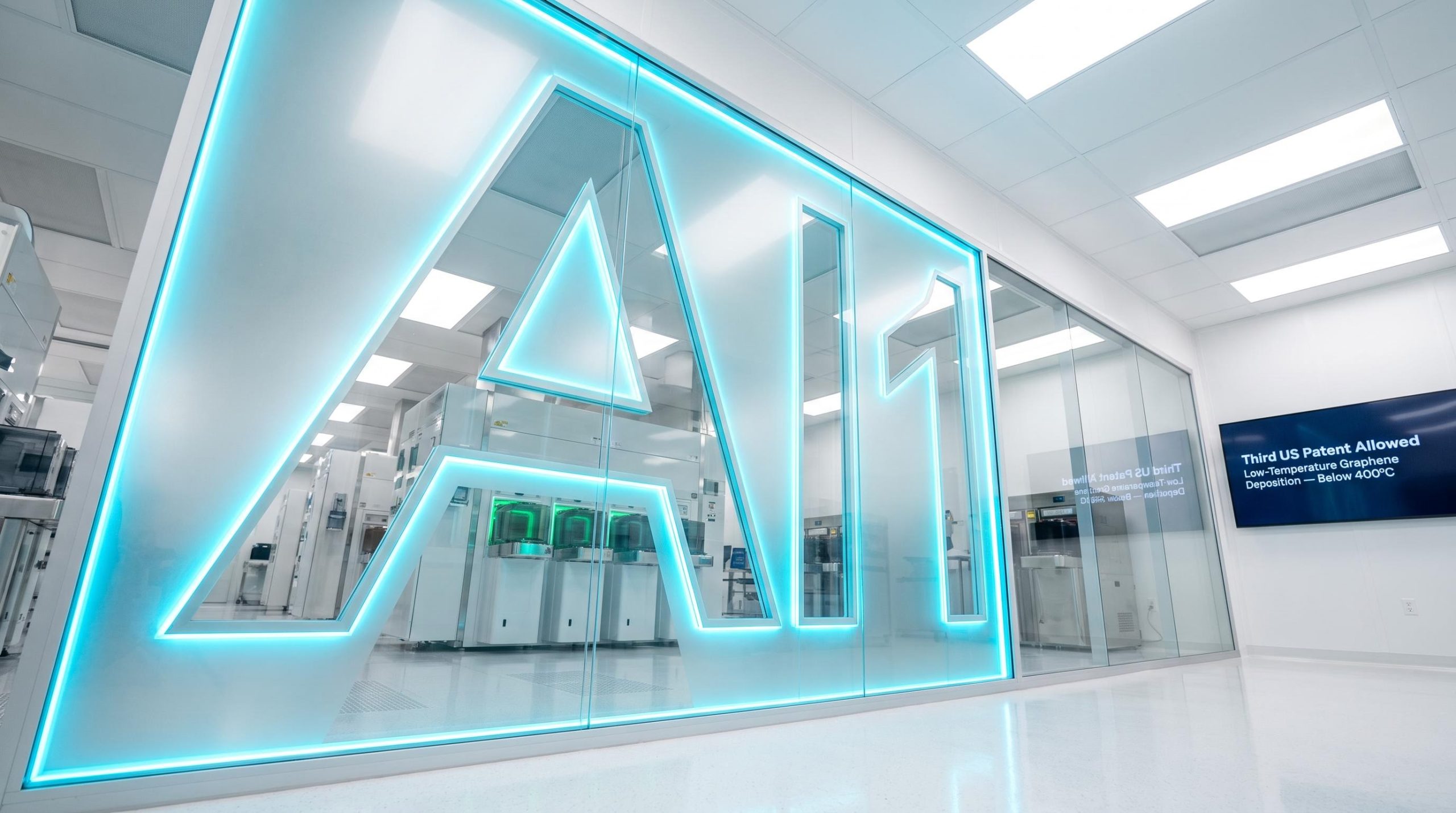
Third US patent allowed, completing both sides of the barrier interface
The United States Patent and Trademark Office (USPTO) has allowed Adisyn Ltd (ASX: AI1) a third US patent, extending the company’s graphene IP coverage to non-metallic surfaces. US Patent Application No. 18/574,061, titled Method for Coating a Non-Metallic Surface with Graphene, complements the two earlier allowed patents covering metallic surfaces and metal-based interconnect products, giving Adisyn protection across both sides of the semiconductor interconnect barrier interface.
Where the prior patents (referenced in ASX announcements dated 7 May 2026 and 31 July 2026) addressed graphene deposition onto metallic surfaces, this third patent protects a method for depositing graphene directly onto non-metallic (dielectric) surfaces. The allowed claims cover a low-temperature process maintained below 400°C throughout, with built-in quality verification via Raman Scattering, Contact Angle Measurement, and Fluorescence Detection. Claims also extend to interconnect structures in which graphene functions as a diffusion barrier between the conducting wire and the surrounding dielectric layer, including along sidewalls.
Kevin Crofton, Executive Chairman
“Our earlier patents protect graphene’s role on the metal side of an interconnect and the granting of our third patent now protects our intellectual property on the barrier interface. … Combined with our other two allowed US patents, we now have a strong, complementary intellectual property position as we continue to advance commercialisation of this breakthrough technology.”
When big ASX news breaks, our subscribers know first
How semiconductor interconnects work — and why the barrier layer matters
Modern chips rely on an intricate stack of materials to transmit electrical signals while preventing interference and contamination. Understanding that stack helps explain why IP coverage on the non-metallic side of the interface carries commercial weight.
Breaking down the interconnect stack
A typical semiconductor interconnect consists of three functional layers:
- Copper wiring — transmits electrical signals across the chip
- Barrier layer (typically tantalum nitride) — stops copper atoms migrating into the surrounding insulating material, which would contaminate and degrade chip performance
- Dielectric layer — acts as a bulk insulator surrounding the copper and barrier layer, made primarily of non-metallic materials
As chip architectures shrink below 5 nanometres (nm), the physical spacing for wiring is reduced to very fine levels. The barrier and dielectric layers, however, cannot be scaled down indefinitely — they must remain thick enough to maintain chip integrity. The result is an increasing proportion of chip real estate devoted to electrical containment rather than transistors, a phenomenon described in the announcement as the “barrier tax.”
Adisyn has demonstrated it is capable of depositing graphene at approximately 1nm thickness (per ASX announcements dated 20 April 2026, 9 June 2026, and 5 August 2026 — writers should verify current status against those filings). Replacing traditional barrier materials with a graphene-based equivalent at that thickness could reduce the barrier tax, potentially enabling more transistors per chip in next-generation architectures. This is precisely why IP coverage on the dielectric (non-metallic) side of the interface carries commercial relevance.
What three complementary patents mean for Adisyn’s IP position
The strategic value here is cumulative. Each individual patent addresses a distinct surface type or application, but together they give Adisyn protection across both sides of the semiconductor interconnect barrier interface, covering the full boundary where copper wire meets dielectric insulation.
Notably, the Executive Chairman confirmed this third patent is built on one of Adisyn’s earliest priority filings, signalling the depth of platform planning from inception.
IP coverage at a glance
⚠️ The exact patent application numbers and filing dates for the first two patents are referenced in the source announcement via the 7 May 2026 and 31 July 2026 ASX announcements but are not reproduced in full in this announcement. The table below reflects what is verifiable from the current source. Writers should cross-reference those filings to complete columns 1 and 3 before publication.
| Patent reference | Surface type covered | Key claim focus | Status |
|---|---|---|---|
| Announced 7 May 2026 & 31 July 2026 (refer to source filings for application numbers) | Metallic | Graphene deposition onto metallic surfaces and metal-based interconnect products | Allowed |
| US Application No. 18/574,061 (announced 14 September 2026) | Non-metallic (dielectric) | Graphene deposition onto non-metallic surfaces; graphene as diffusion barrier between conducting wire and dielectric layer, including sidewalls; low-temperature process below 400°C | Allowed |
The combined patent position now protects:
- Graphene deposition onto metallic surfaces
- Metal-based interconnect products
- Graphene deposition onto non-metallic (dielectric) surfaces
- Graphene as a diffusion barrier between the conducting wire and the surrounding dielectric layer, including along sidewalls
- A low-temperature deposition process (below 400°C) applicable across the portfolio
What comes next for Adisyn
The announcement does not disclose specific commercialisation milestones or timelines. The company’s stated direction is continuing to advance commercialisation of its low-temperature graphene deposition technology, with the IP portfolio now protecting multiple angles of application in next-generation semiconductor manufacturing.
Adisyn operates across several technology streams. Its core focus is the development of its low-temperature Atomic Layer Deposition (ALD) process for semiconductor interconnect applications. The company is also exploring graphene-based composite materials designed to reduce radar signatures in UAV and defence platforms, alongside Adisyn Services, which provides managed IT, cloud, cybersecurity, and artificial intelligence solutions to Australian small and medium-sized enterprises.
With IP now covering both the metallic and non-metallic sides of the interconnect barrier interface, the company holds a more complete foundation from which to pursue its commercialisation objectives in advanced semiconductor manufacturing.
Investors exploring the scale-up trajectory behind the deposition technology will find our full explainer on Adisyn’s 200mm wafer milestone covers the 300x area expansion from coupon to full wafer, the independent verification methodology used at the Hebrew University of Jerusalem, and what the 300mm wafer target means for commercial fab compatibility.
Don’t Miss the Next ASX Tech Breakthrough
Get FREE breaking ASX tech news delivered to your inbox within minutes of release, complete with in-depth analysis. Join 20,000+ investors already staying ahead of the market with Big News Blast. Click the “Free Alerts” button to receive the moment market-moving technology announcements hit the ASX.