
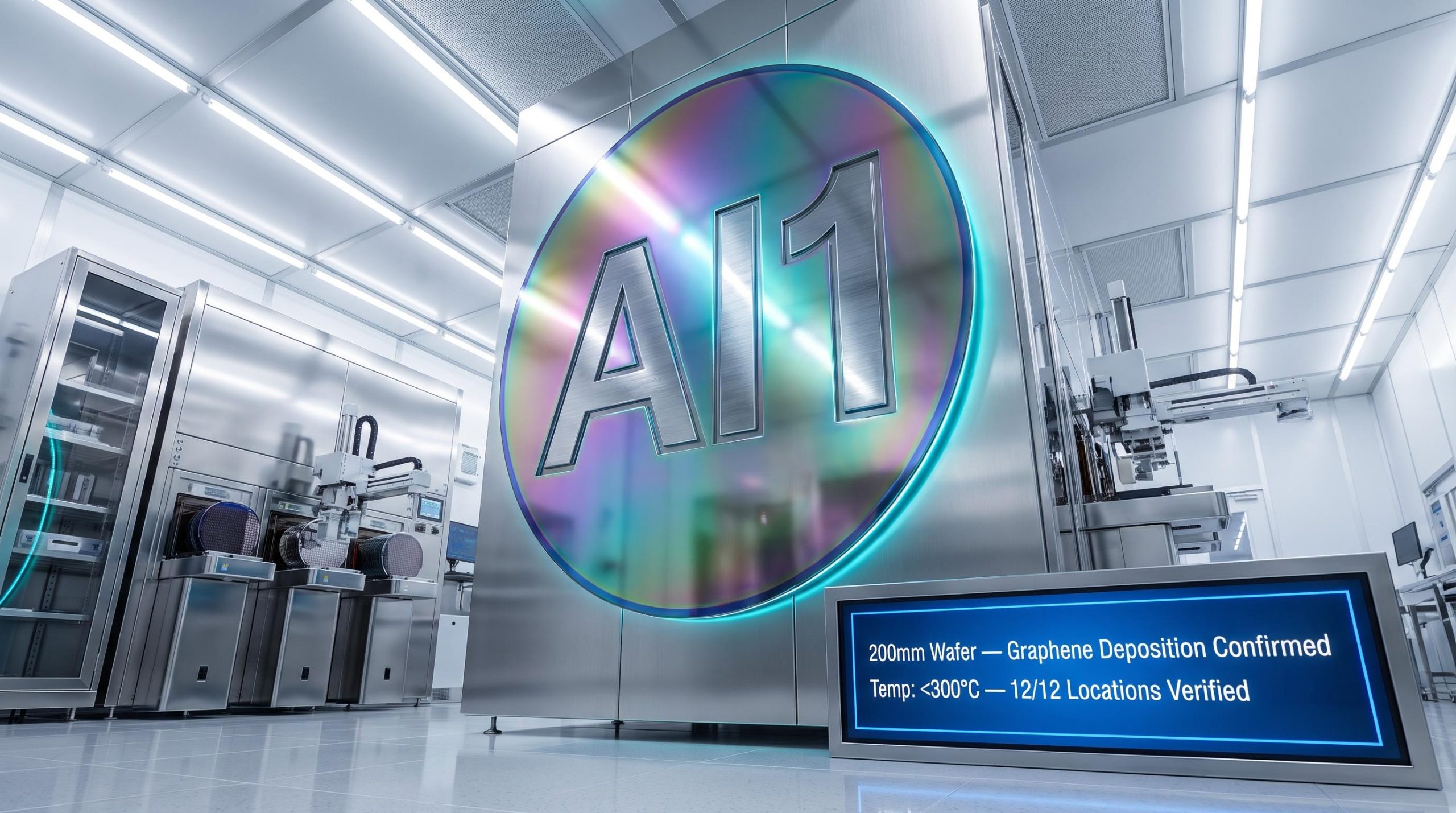
Adisyn scales graphene deposition to full 200mm wafer in industry first
Adisyn Ltd (ASX: AI1) has successfully deposited low-temperature graphene across a full 200mm semiconductor wafer, the industry-standard format used across global chip manufacturing. According to the company, this is the first publicly disclosed demonstration of low-temperature graphene deposition across an entire 200mm wafer.
The deposition was completed below 300°C on a wafer surface of approximately 314cm², roughly 300 times the area of the previously announced 1cm² coupon. The company noted the result was achieved significantly ahead of internal development expectations.
When big ASX news breaks, our subscribers know first
What the milestone means for Adisyn’s semiconductor program
The transition from a lab-scale coupon to an industry-standard wafer marks a substantial scale-up of the technology platform. Adisyn stated the achievement validates its process at a format widely used throughout commercial semiconductor manufacturing.
The 200mm wafer result builds directly on graphene deposition on industrial ALD equipment first demonstrated at coupon scale, where Adisyn confirmed continuous graphene growth below the 450°C thermal ceiling required for compatibility with existing commercial fabrication facilities.
The result provides a platform for device-integration testing, prospective industry joint development programs and progression towards the 300mm wafer formats used in advanced AI, high-performance computing and memory devices. For investors, the ahead-of-schedule milestone strengthens the technical foundation underpinning planned industry collaboration.
Arye Kohavi, Managing Director
“This is a huge step forward for Adisyn and a strong demonstration of the speed at which our graphene semiconductor technology is advancing. Scaling a new materials technology from laboratory samples to a full 200mm semiconductor wafer presents significant technical challenges. Achieving that step – and identifying graphene at all 12 locations independently tested across the wafer – provides important validation of our technology and development approach. Complete industrial wafer coverage is a critical goal that the company expected to achieve in just a few months, and meeting it today shortens the planned timelines for industry collaborations and integrations.”
How the result was independently verified
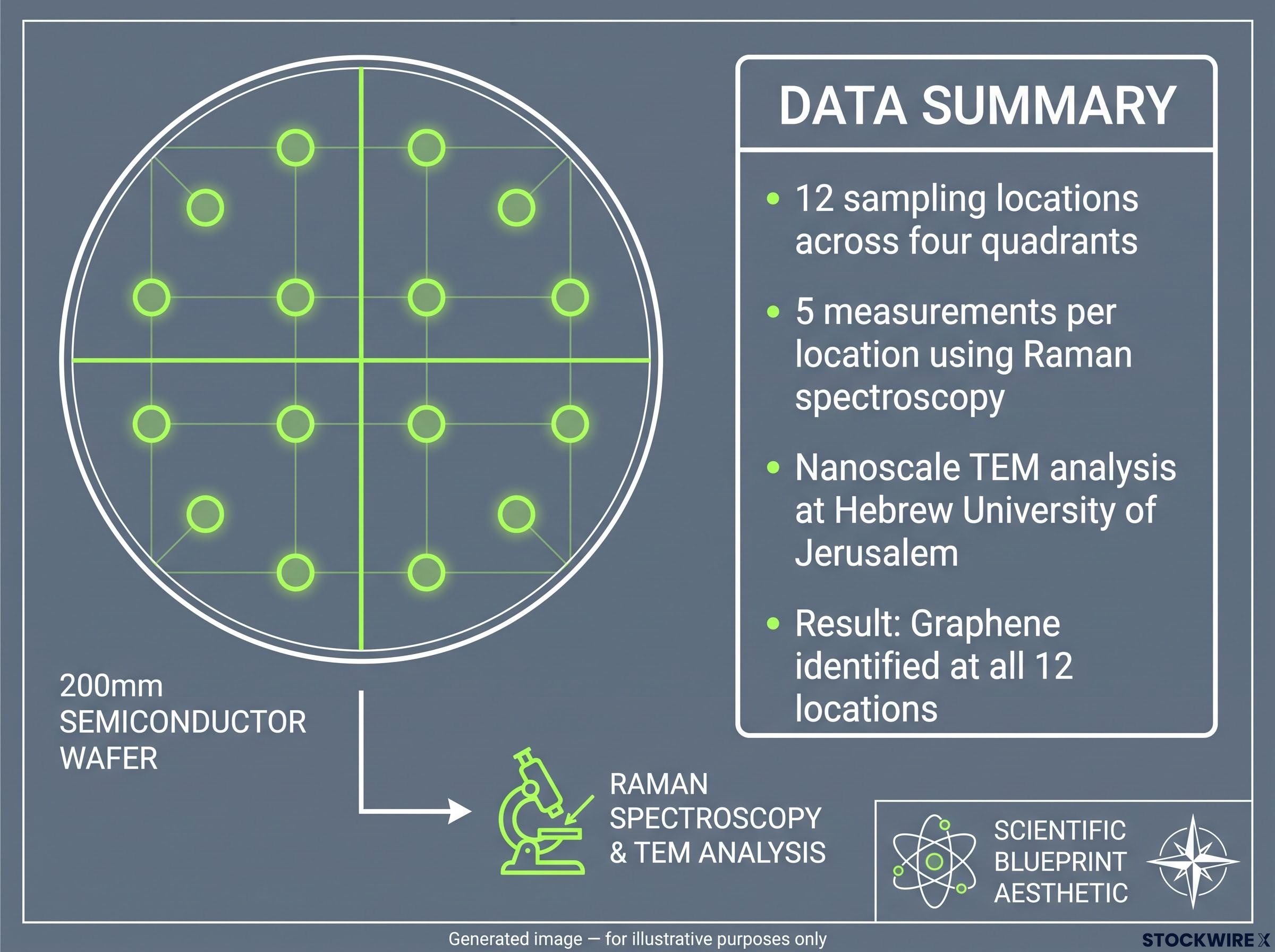
The credibility of the milestone rests on independent, multi-point testing conducted after deposition. The verification methodology included:
-
12 sampling locations selected across all four quadrants and at varying distances from the wafer centre
-
Each location measured five times using Raman spectroscopy
-
Complementary nanoscale analysis via Transmission Electron Microscopy (TEM) at the Hebrew University of Jerusalem
-
Graphene identified at all 12 locations
Raman spectroscopy was used to identify and characterise the deposited graphene, while TEM provided complementary nanoscale analysis. The independent, multi-point confirmation strengthens confidence for prospective joint development partners.
| Metric | Previous (Coupon) | New (200mm Wafer) | Significance |
|---|---|---|---|
| Coated area | 1cm² | ~314cm² | ~300x increase in a single run |
| Format | Lab coupon | Industry-standard 200mm wafer | Commercial relevance |
| Deposition temperature | — | Below 300°C | Low-temperature process |
| Verification points | — | 12 locations, all confirmed | Independently validated |
Why graphene matters in next-generation chips
Graphene is being investigated internationally for semiconductor interconnects and for hybrid graphene-metal structures.
The material addresses a growing problem: the performance limitations of copper interconnects as chip structures continue to shrink. These constraints are particularly relevant to advanced AI, high-performance computing and memory devices.
Such advanced devices are predominantly manufactured on 300mm wafers. That makes Adisyn’s 200mm result an important pathfinder towards achieving the larger format, positioning the company within a globally significant, high-value materials problem.
The commercial pathway from here
Adisyn believes successful integration of its process technology platform will create commercial opportunities through “potential licensing, joint-development, process or materials-supply models.” The company has cautioned that further development, device integration and customer qualification are required, and it has not provided revenue or earnings forecasts.
Underpinning the commercial pathway is a US patent covering its graphene coating method, resulting products and devices, with the granted IP establishing defect density thresholds and surface coverage specifications that differentiate the technology from competing approaches.
The next phase of development, as outlined by the company, includes:
-
Refine and repeat the deposition process to assess uniformity, defectivity and reproducibility
-
Determine initial first-pass reliability data across various applications
-
Advance technical engagement with prospective semiconductor industry partners
-
Evaluate opportunities to integrate the technology into semiconductor development programs
-
Progress work directed towards larger 300mm wafer formats
What it means for investors
The independently verified, ahead-of-schedule milestone at industry-standard scale gives Adisyn a stronger foundation from which to pursue joint development programs with semiconductor manufacturers. The company stated it will provide further updates as material technical and commercial milestones are achieved.
Beyond its semiconductor focus, Adisyn is also developing graphene composites aimed at reducing radar signatures in UAV and defence platforms, and operates Adisyn Services, providing managed IT, cloud, cybersecurity and AI solutions to Australian small and medium-sized enterprises.
Don’t Miss the Next ASX Tech Breakthrough
Big News Blast delivers FREE breaking ASX tech news directly to your inbox within minutes of release, complete with in-depth analysis. Join 20,000+ subscribers already staying ahead of the market. Click the “Free Alerts” button at StockWire X to get the next market-moving announcement the moment it drops.