Morningstar vs Markets: a 125-Point Gap in the US Rate Outlook
39 mins ago
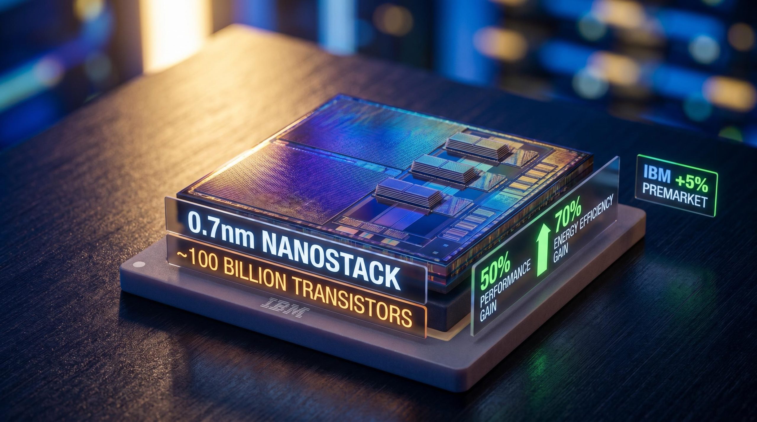
IBM has demonstrated a chip operating below one nanometre, a threshold the semiconductor industry has long treated as a hard physical wall. The company’s stock climbed around 5% in premarket trading on 25 June 2026, following the announcement.
The announcement, made at the VLSI 2026 conference, introduces a 3D nanostack transistor architecture rather than a conventional node shrink. The distinction matters enormously for how to read the move. Packing transistors at close to twice the density of IBM’s 2nm chip, and delivering performance and efficiency gains that address AI and data-centre bottlenecks directly, the 0.7nm nanostack is a credible technical achievement. Whether it is a credible investment catalyst is a different question.
This piece tells you whether that 5% premarket spike reflects something durable or something that tends to fade, what specific signals would change that assessment, and how to frame the IBM chip breakthrough within the company’s actual monetisation model.
The 0.7nm designation puts this chip in territory below the one-nanometre threshold, a node class that had not been realised in functioning silicon before now despite years of industry pursuit. The number is architecturally significant, not just numerically impressive, because conventional transistor designs lose the ability to control current flow reliably at these dimensions.
IBM’s solution is structural. The nanostack vertically stacks CMOS nanosheet channels into separate “top” and “bottom” devices, each with independently optimised geometry and materials. That vertical layering, distinguishing the design from both planar transistors and single-stack gate-all-around architectures, is what allows it to pack far more devices into the same footprint while maintaining electrostatic control.
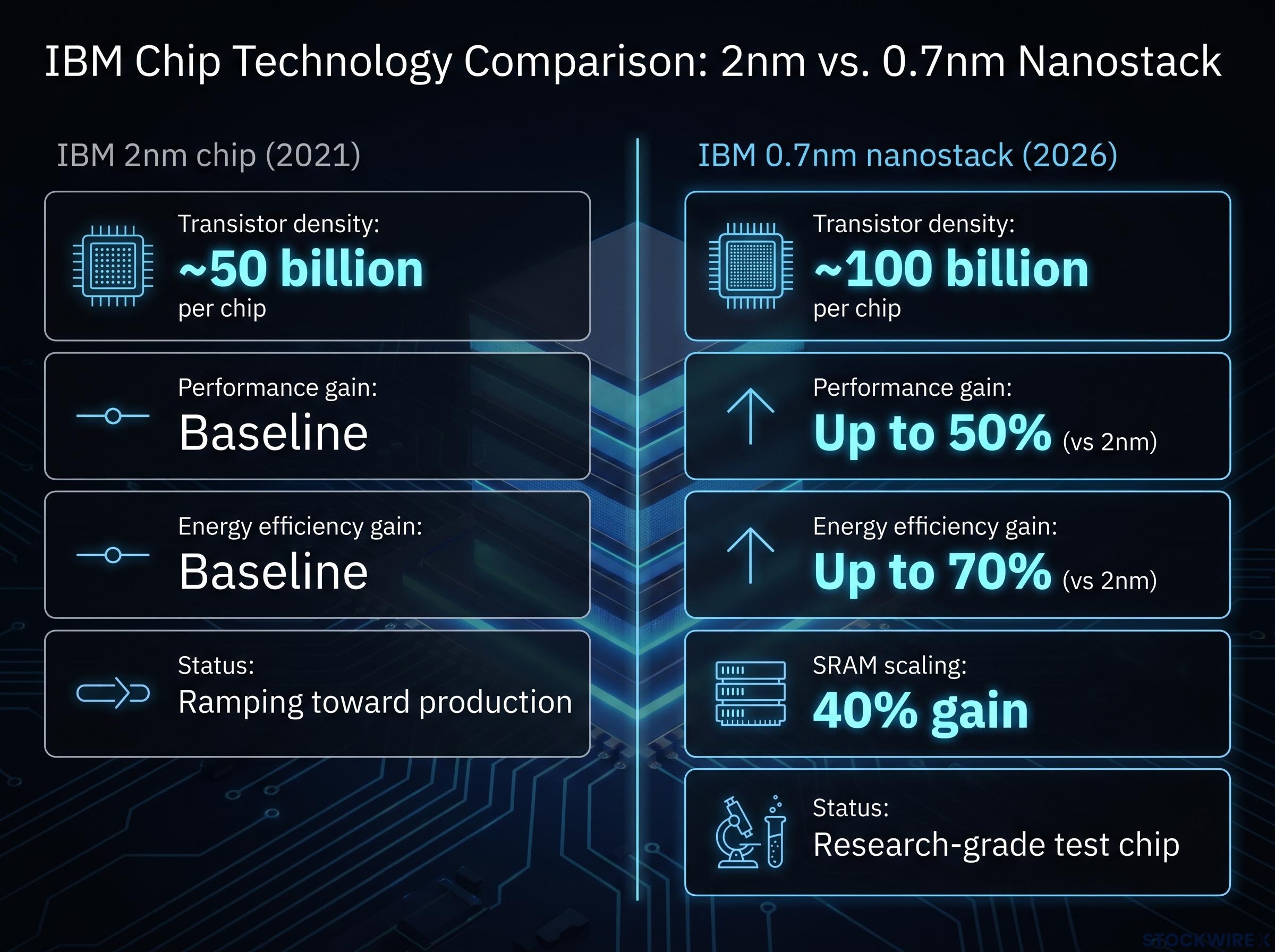
Transistor density: close to 100 billion transistors packed into a chip roughly the size of a fingernail.
This is a research-grade test chip demonstrated at a conference, not a finished commercial processor. The performance metrics below describe what the architecture can achieve under lab conditions. Historically, lab-condition gains at this stage of development narrow before they reach a production line; these figures represent a ceiling to calibrate against, not a guarantee of shipped performance.
| Attribute | IBM 2nm chip (2021) | IBM 0.7nm nanostack (2026) |
|---|---|---|
| Transistor density | ~50 billion per chip | ~100 billion per chip |
| Performance gain (vs 2nm) | Baseline | Up to 50% |
| Energy efficiency gain (vs 2nm) | Baseline | Up to 70% |
| Status | Ramping toward production | Research-grade test chip |
Technical results presented at VLSI 2026 showed the nanostack architecture achieving a 40% gain in SRAM scaling, adding further weight to the density case. These numbers give you the vocabulary to assess coverage without relying on headline hype.
As transistors shrink below conventional limits, the gate (the component that switches the transistor on and off) loses its ability to control current flow through the channel beneath it. Electrons begin to leak through pathways the gate cannot reach, degrading performance and wasting power. Standard planar architectures hit this wall hard; even single-stack gate-all-around designs face diminishing returns at the dimensions IBM is targeting.
The nanostack addresses that problem through geometry. Three structural properties set it apart:
The combination of high drive current with tight electrostatic control is precisely what power-constrained AI inference and training workloads demand. Data-centre power consumption is becoming a commercially binding constraint for hyperscalers and cloud providers. A transistor architecture that delivers substantially more performance per watt addresses a problem that is getting more commercially urgent every year, which is a meaningful difference from a specification improvement without a clear demand driver.
Custom AI chip economics have made data-centre power consumption a commercially binding constraint: hyperscalers building proprietary ASICs cite energy efficiency per inference as the primary design target, which is precisely the metric IBM’s nanostack architecture improves most aggressively over the 2nm baseline.
IBM is no longer a volume merchant foundry. It develops process technology and device architectures, then monetises through partners and licensing. That means the commercialisation timeline depends on manufacturing decisions made by other companies, not by IBM itself.
The 2nm precedent is instructive. IBM announced that test chip in 2021, with a multi-year ramp toward volume production targets. As of mid-2026, that node is still working its way into real-world product portfolios. The gap from lab demonstration to large-scale deployment has been consistently measured in years, not quarters.
For the 0.7nm nanostack, the infrastructure is still being built. In March 2026, IBM and Lam Research entered a five-year collaboration to develop new materials and processes, including high-NA EUV patterning, aimed explicitly at sub-1nm logic scaling. Neither company named a manufacturing partner or gave a production timeline. Rapidus in Japan is frequently mentioned in industry commentary as a potential mass-production partner for IBM-developed process technologies, though no concrete sub-1nm production plans have been publicly confirmed.
The Lam Research collaboration is specifically structured around high-NA EUV lithography, the patterning technology that enables single-exposure printing at the feature sizes sub-1nm logic demands, replacing multi-patterning steps that represent the largest cost and throughput constraint at leading-edge nodes.
The commercialisation sequence looks like this:
The commercialisation window for this architecture is a late-decade story at best, not a 2026-2028 revenue event.
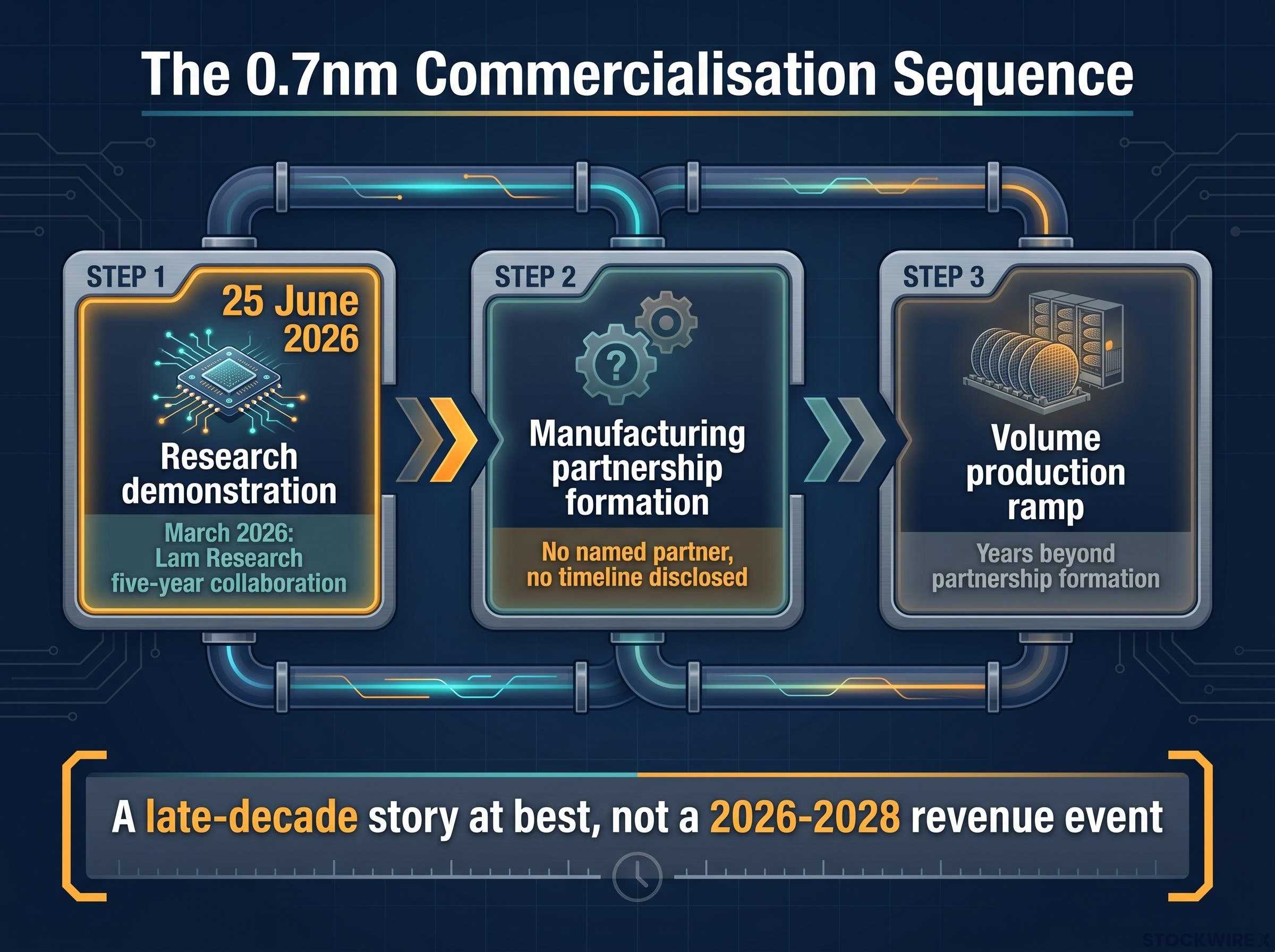
That framing is not pessimistic. It simply means the 5% premarket move is priced on narrative, not on an imminent earnings line.
The question most coverage misses is whether IBM needs to manufacture this chip itself to extract value from it. The answer is no, and that changes the risk profile considerably.
IBM’s model is IP-and-partnership. The company creates process and device architecture intellectual property, then monetises through three channels:
The Lam Research collaboration is structured explicitly to marry IBM’s device and integration expertise with Lam’s process tool and materials capabilities for sub-1nm logic. It is the template for how IBM intends to move nanostack from research to revenue without bearing the capital burden of building a leading-edge fab.
Sub-1nm R&D aligns directly with ongoing US, EU, and Japanese efforts to secure domestic access to next-generation logic nodes. The CHIPS Act investment climate in the US, along with equivalent programmes in Japan and Europe, means partnerships built on IBM IP can attract public funding. That de-risks IBM’s R&D spending and creates value for shareholders without equity dilution.
CHIPS Act subsidies have already demonstrated their ability to accelerate partnership formation in the foundry sector, with $14.9 billion in combined commitments to Intel and Samsung facilities shifting the calculus for any manufacturer considering a domestic sub-1nm production investment alongside IBM IP.
The investor implication is direct: IBM does not need to build a leading-edge fab to extract value from nanostack. It needs to land one or two meaningful licensing or joint venture deals, a fundamentally lower-risk and lower-capex path to return than competing on fab utilisation.
IBM’s current revenue is dominated by software, hybrid cloud, and consulting. None of that changes with this announcement. The 5% premarket move is best understood as the market pricing sentiment and long-term optionality, not an earnings inflection.
That optionality argument is legitimate for long-duration holders. But without follow-on catalysts, this kind of sentiment-driven move has a historical tendency to mean-revert. The 2nm precedent supports that reading: the initial excitement around a research milestone gave way to the slower reality of multi-year commercialisation timelines.
The specific signals that would justify a more durable re-rating are concrete and observable:
For an investor deciding whether to act on today’s move, this is a watchlist addition with defined triggers, not a catalyst to chase before those triggers materialise.
Two investor horizons, two different readings. Long-term holders with a 3-7 plus year view gain a genuine incremental reason to remain constructive on IBM’s IP-and-ecosystem thesis. The nanostack work compounds the company’s credibility as a pathfinder in advanced logic, a role that builds bargaining power slowly but carries lower execution risk than merchant foundry competition.
Short-term traders face a mean-reversion risk. Without the catalysts outlined above, there is no near-term earnings attach point for this announcement.
Three things changed today, and one thing did not:
The nanostack announcement is not the inflection point itself. It is evidence that IBM is building toward one, and the four catalyst triggers above are how you will know when it arrives.
For investors wanting to place IBM’s nanostack within the broader long-duration semiconductor thesis, our full explainer on the AI semiconductor sector outlook covers BofA’s $2.7 trillion industry revenue projection and the specific sub-sectors — memory, accelerators, and wafer fab equipment — driving the forecast through 2030.
This article is for informational purposes only and should not be considered financial advice. Investors should conduct their own research and consult with financial professionals before making investment decisions. Past performance does not guarantee future results. Forward-looking statements regarding commercialisation timelines and partnership developments are speculative and subject to change based on market developments and company performance.
IBM's 0.7nm nanostack is a research-grade chip that vertically stacks CMOS nanosheet channels into separate top and bottom devices, each independently optimised, allowing roughly 100 billion transistors to be packed into a fingernail-sized chip while maintaining full gate-all-around electrostatic control.
IBM shares climbed around 5% in premarket trading on 25 June 2026 after the VLSI 2026 announcement, a move that reflects the market pricing long-term narrative optionality rather than any change to IBM's 2026-2028 earnings trajectory.
No manufacturing partner or production timeline has been publicly confirmed; IBM's own 2nm chip, announced in 2021, is still working into real-world product portfolios as of mid-2026, making the 0.7nm nanostack a late-decade commercialisation story at best.
IBM monetises through licensing transistor and integration IP to foundries, cost-sharing joint R&D programmes with equipment vendors (such as its five-year collaboration with Lam Research), and pulling the technology into its own Power, mainframe, and AI accelerator products manufactured by partners.
The clearest signals are: a named foundry or national champion committing to pilot production, integration of nanostack into IBM's own product roadmaps with indicative timing, and licensing or joint venture deals that attach dollar figures or minimum-volume commitments to IBM's sub-1nm IP portfolio.