APRA Makes Geopolitical Risk Readiness a Supervisory Obligation
5 hrs ago
A single fabrication process announcement sent Intel shares up roughly 4% in premarket trading on 17 June 2026, and pulled most of the semiconductor sector higher with it. The news: Intel’s 18A-P node has entered risk production, a milestone disclosed at the 2026 VLSI Symposium that confirms the company’s foundry turnaround is, for now, running on schedule.
The timing carries weight. AI infrastructure spending is driving acute demand for chips that deliver better performance per watt, and Intel’s ability to manufacture them competitively is the single largest variable in its financial recovery thesis. What follows explains what the 18A-P process node actually delivers technically, why risk production matters beyond a press release, and how investors should interpret both the Intel-specific and sector-wide market moves that followed.
Intel 18A-P is not a new node built from scratch. It is a performance-optimised enhancement to the baseline Intel 18A process, built on the same RibbonFET gate-all-around transistors and PowerVia backside power delivery architecture. The gains come from coordinated transistor, interconnect, and design-technology co-optimisation improvements layered on top of that foundation.
The headline metrics, disclosed at the 2026 VLSI Symposium and corroborated by Tom’s Hardware, tell a clear story.
Intel Foundry’s VLSI Symposium disclosure confirmed the specific performance figures underpinning the 18A-P announcement, including the 20-40% thermal resistance improvement and the via resistance gains that contribute to the node’s power efficiency profile.
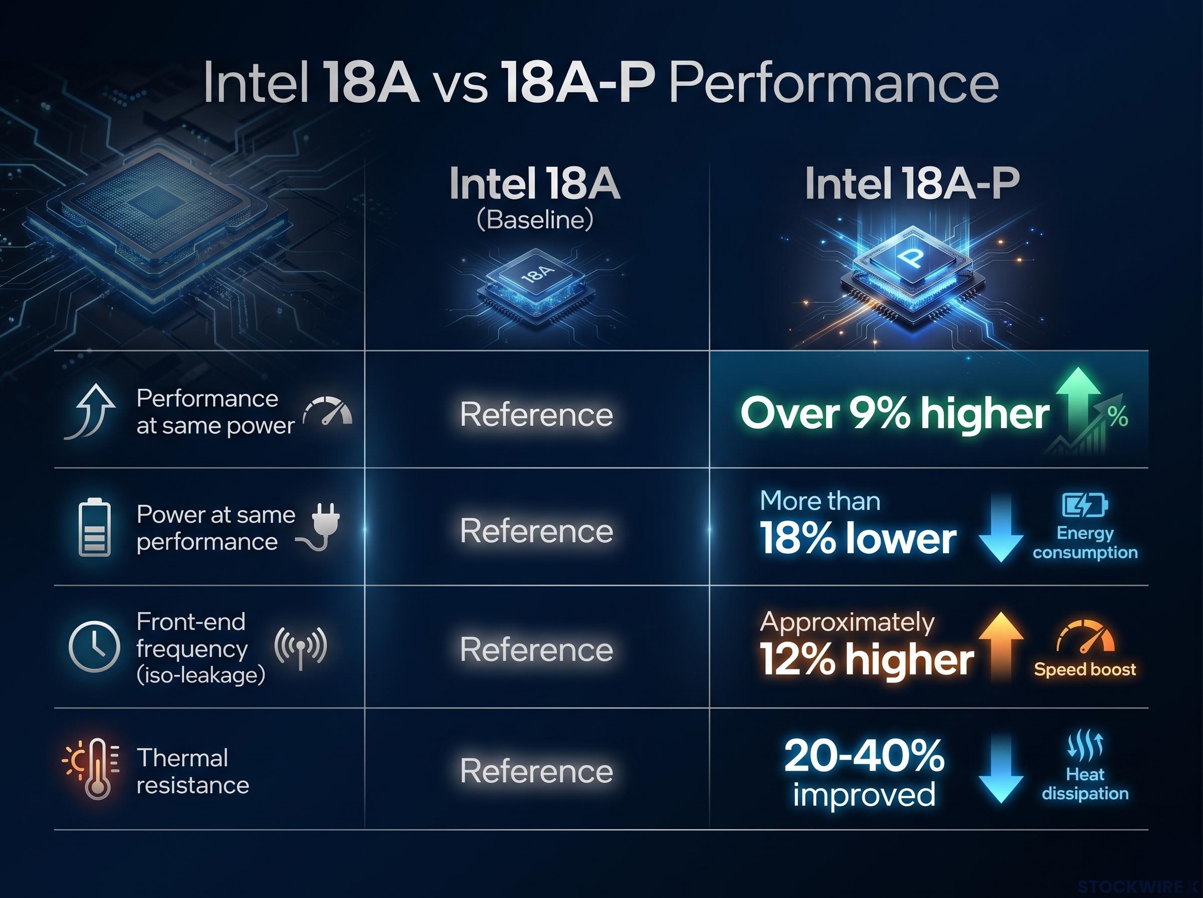
| Attribute | Intel 18A (Baseline) | Intel 18A-P |
|---|---|---|
| Performance at same power | Baseline | Over 9% higher |
| Power at same performance | Baseline | More than 18% lower |
| Front-end frequency (iso-leakage) | Baseline | Approximately 12% higher |
| Thermal resistance | Baseline | 20-40% improved |
Those numbers are harder to achieve than they appear. At this transistor scale, single-digit percentage gains in performance or power require changes across multiple layers of the manufacturing stack simultaneously.
The gains Intel is reporting at 18A-P sit within a broader reshaping of advanced chip manufacturing economics, where lithography improvements, transistor architecture changes, and backside power delivery are each contributing incremental efficiency gains that compound across the manufacturing stack.
Beyond the headline specifications, 18A-P introduces Power Boost RibbonFET transistor options that support higher drive current. For chip designers targeting high-performance computing (HPC) and AI workloads, this translates into greater design flexibility at the transistor level.
The commercially meaningful detail: 18A-P retains identical design rules to baseline 18A. Fabless customers already evaluating Intel’s platform can reuse existing intellectual property and design flows, reducing non-recurring engineering (NRE) costs and shortening time-to-market.
What is risk production? Risk production is the phase in which a semiconductor process is run on real hardware to validate that it can be manufactured reliably before volume production begins. It tests whether the process works at scale, not whether it can ship commercially.
The distinction matters. Risk production is not a revenue event. It is a credibility event. Intel told customers in 2025 that 18A-P would reach this stage by mid-2026, and it has. Hitting a publicly committed roadmap milestone on schedule is the most direct form of execution evidence the company can provide ahead of volume ramp.
The roadmap ahead follows a defined sequence:
Volume production timelines will determine when foundry revenue begins flowing. Risk production confirms the process works; volume ramp determines whether it pays.
The premarket moves on 17 June 2026 were broad, but the causal logic behind them was not uniform.
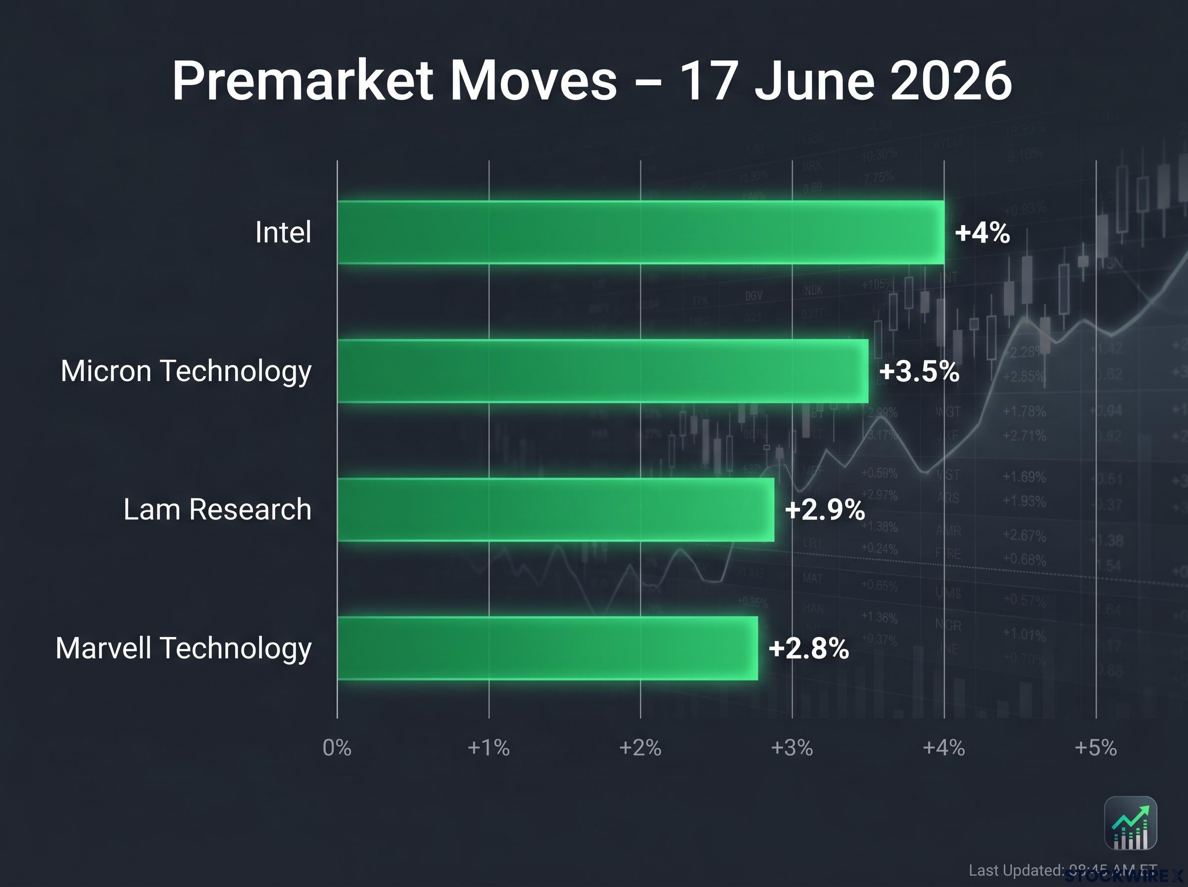
| Company | Premarket Move (Approx.) | Ecosystem Role |
|---|---|---|
| Intel | +4% | Foundry operator, chip designer |
| Micron Technology | +3.5% | Memory manufacturer |
| Lam Research | +2.9% | Semiconductor equipment supplier |
| Marvell Technology | +2.8% | Custom silicon designer (data centres) |
Attribution note: Premarket figures sourced from Investing.com reporting by Sam Boughedda, published 17 June 2026. Premarket data is not preserved in standard archives in the same manner as closing prices.
Intel’s move was directly tied to the 18A-P announcement. The peer moves are better characterised as improved sentiment toward the semiconductor complex. The sector had declined in the prior session on 16 June 2026, and the premarket recovery reflected a partial rebound alongside a specific catalyst.
The distinction matters for portfolio decisions. A fabrication node announcement moving suppliers, memory makers, and fabless designers simultaneously can reflect genuine shared tailwinds or contagious sentiment. In this case, the evidence points to both operating at once.
Sector-wide semiconductor sector risk factors extend well beyond individual node milestones: geopolitical export policy, China revenue exposure at Nvidia and TSMC, and the asymmetric downside that Bloomberg Intelligence estimated at 10-20% for the SOXX on a hardline summit outcome represent the macro overlay within which Intel’s foundry story is playing out.
An 18% power reduction at the process level sounds like an engineering benchmark. For hyperscalers operating large-scale AI clusters, it is a dollar figure.
At data-centre scale, even mid-single-digit improvements in chip-level power efficiency can translate into tens of millions of dollars annually in energy and cooling savings. The 18A family targets precisely the workloads where this arithmetic dominates procurement decisions: AI accelerators, HPC, and data-centre CPUs.
The scale of hyperscaler AI capital expenditure, with Amazon, Microsoft, Alphabet, and Meta collectively spending $130 billion in Q1 2026 alone, is what converts a process node power efficiency number into a procurement criterion worth billions in annual energy and cooling savings.
Lawrence Berkeley National Laboratory projections estimate that U.S. data centres could consume between 9% and 17% of total domestic electricity demand by 2030, driven primarily by AI workload growth, a trajectory that makes chip-level power efficiency gains directly material to infrastructure operating costs.
Hyperscaler procurement teams evaluate process nodes against three primary criteria:
The 20-40% improvement in thermal resistance compounds the power efficiency gains. Lower thermal output per chip means denser server rack configurations, which reduces the physical footprint of AI clusters.
Design-rule compatibility with baseline 18A lowers the barrier for customers already evaluating Intel’s foundry platform. A customer that has begun IP development on 18A can transition to 18A-P without significant rework, a commercial advantage that reduces switching cost calculations.
Marvell Technology, as a designer of custom silicon for data centres and networking infrastructure, illustrates the type of customer for whom these economics are directly relevant. No public confirmation of a specific Intel 18A-P foundry engagement exists, but Marvell’s position in the AI data-centre supply chain makes it a strategically significant name to monitor.
The 18A-P milestone earns Intel genuine technical credibility. Technical analyses suggest the 18A family offers competitive performance-per-watt characteristics relative to TSMC’s most advanced nodes. That is not a trivial achievement for a company that trailed the leading edge for most of the past decade.
The structural gap between technical credibility and commercial market share remains wide.
TSMC’s capacity advantage at the leading edge is structural rather than cyclical: at 3nm, TSMC is targeting approximately 180,000 wafers per month by end-2026, roughly eight times the estimated output at both Samsung and Intel, a production scale gap that cannot be closed through a single node improvement regardless of how competitive that improvement’s specifications appear.
Intel earning the right to compete for foundry business is different from winning it. TSMC’s market position rests on ecosystem relationships and an execution track record that Intel has not yet matched at volume scale.
Intel remains loss-making on a trailing twelve-month basis as of mid-2026, with advanced-node foundry revenue identified as a key swing factor for a projected return to profitability. The financial stakes attached to converting technical milestones into commercial wins are not abstract.
The 18A-P risk production entry confirms manufacturability. What determines whether the premarket optimism translates into durable thesis validation is the sequence that follows.
Three forward-looking checkpoints, in order of importance:
Volume ramp execution matters more than risk production as a financial signal. Risk production validates that the process works; volume ramp determines when foundry revenue materialises and at what margin.
Intel’s stock had already posted significant gains in recent trading sessions ahead of the 17 June announcement. Investors assessing the premarket move should weigh how much of the positive news was already reflected in the price before the formal disclosure.
The 18A-P risk production milestone is a genuine technical and roadmap credibility achievement. Intel met a publicly committed timeline, disclosed competitive specifications, and demonstrated that its foundry turnaround is progressing through defined manufacturing gates.
The sector-wide premarket move reflects legitimate AI infrastructure tailwind sentiment. Intel’s specific move reflects execution evidence against a financial recovery thesis that remains unproven at commercial scale.
Sustained stock performance will depend on volume ramp execution and external customer announcements, not additional specification disclosures. The engineering case has advanced. The commercial case has not yet been made.
This article is for informational purposes only and should not be considered financial advice. Investors should conduct their own research and consult with financial professionals before making investment decisions. Past performance does not guarantee future results. Forward-looking statements regarding Intel’s volume production timelines, customer engagements, and financial recovery are subject to change based on market developments and company performance.
Intel 18A-P is a performance-optimised enhancement to the baseline Intel 18A process node, built on the same RibbonFET gate-all-around transistors and PowerVia backside power delivery architecture. It delivers over 9% higher performance at the same power and more than 18% lower power at the same performance, while retaining identical design rules to baseline 18A.
Risk production is the phase in which a semiconductor process is run on real hardware to validate that it can be manufactured reliably before volume production begins. It confirms the process works at scale but is not a revenue event; volume ramp is the subsequent stage that determines when foundry revenue materialises.
Intel shares rose approximately 4% in premarket trading directly tied to the 18A-P risk production milestone, while peers including Micron, Lam Research, and Marvell posted gains of 2.8-3.5%, reflecting improved broader sentiment toward the semiconductor sector alongside a partial rebound from declines in the prior session.
At data-centre scale, even mid-single-digit chip-level power efficiency gains can translate into tens of millions of dollars annually in energy and cooling savings; the 18A-P node's 18% power reduction and 20-40% thermal resistance improvement are therefore evaluated by hyperscaler procurement teams as direct financial criteria, not just engineering benchmarks.
The three key checkpoints are: volume production entry for 18A-P (expected later in 2026), which will make foundry revenue timing and margin recovery quantifiable; confirmed external customer tape-outs on 18A-P, the strongest signal that foundry interest is converting into commercial commitments; and 18A-PT risk production entry, confirming the derivative roadmap is on schedule.