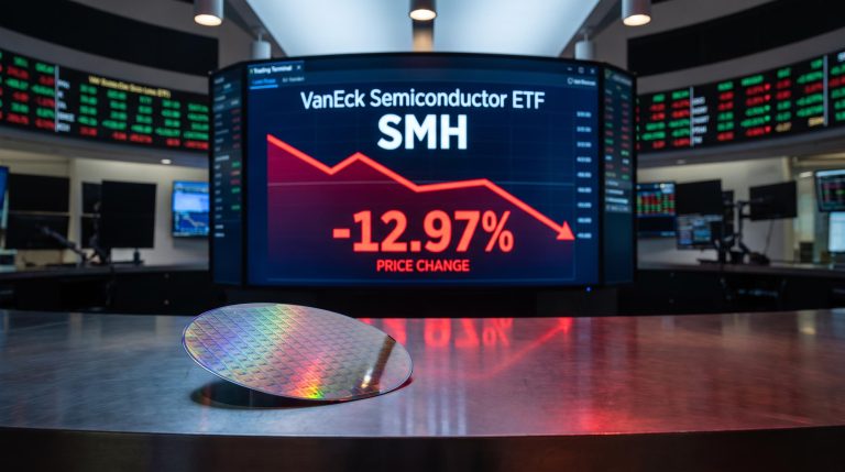
A single anonymously sourced report triggered a sharp semiconductor selloff on 27 July 2026. The headline said China had achieved “mass production” of immersion DUV lithography tools. The underlying numbers told a different story: roughly five machines scheduled for delivery this year, still in qualification, approximately a decade behind ASML’s leading systems.
Geopolitically charged technology claims are now a recurring feature of investing in semiconductors. The investors who lose money on them are typically those who react to the headline. The ones who navigate them well have a repeatable process for separating what the words say from what the data actually supports.
This piece uses the China DUV story as a live case study to show you exactly how to run that process, from interrogating sourcing to stress-testing the numbers to deciding what, if anything, changes in your investment thesis.
What the China DUV report actually claims, and what it does not
The core claim is specific enough to evaluate. A Shanghai state-backed firm, Yuliangsheng Technology, affiliated with SiCarrier and Huawei-linked entities, has begun producing immersion deep-ultraviolet (DUV) lithography scanners. DUV scanners are the machines that print circuit patterns onto silicon wafers, the foundational step in chipmaking. First units are scheduled for delivery to SMIC, Hua Hong, and CXMT, three of China’s largest chipmakers.
Then the production numbers arrive. Approximately five systems in 2026. Approximately 20 in 2027. All still in qualification or early deployment, not industrial-scale output.
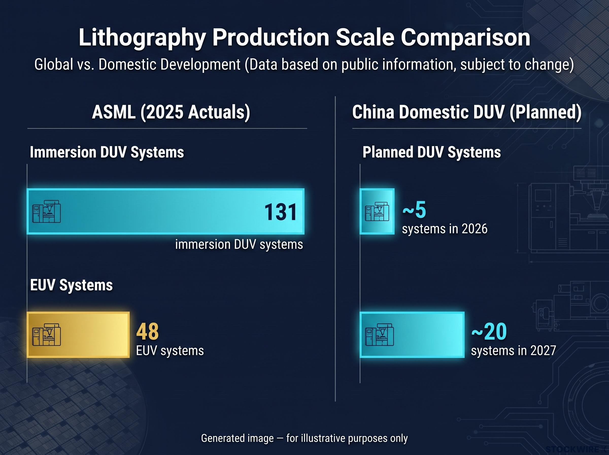
The gap in a single line: headlines described “mass production.” The underlying data describe approximately five qualification-phase tools scheduled for delivery this year.
The sourcing adds a further layer of caution. The Information’s staff-bylined story cited “two people familiar with the programme,” standard for sensitive industrial reporting but limiting independent verification. Tom’s Hardware and others echoed the claim, often relying on the same anonymous sourcing rather than independently corroborating it. Reader commentary on Investing.com (users RSI50 and Abdelmaksoud Khalifa, 27 July 2026) noted that the “mass production” framing appeared to overstate a qualification-stage milestone.
The timing matters too. The report published on 27 July 2026, as the MATCH Act (introduced April 2026, advanced by the House Foreign Affairs Committee) was moving through Congress. A single anonymously sourced story landing during active U.S.-China trade and export-control negotiations should be treated as a hypothesis requiring corroboration, not a confirmed operational fact. The gap between “mass production” and “five qualification-phase tools” is not a minor semantic distinction; it is the difference between a thesis-changing event and a sentiment event.
US-China trade fault lines on Taiwan’s political status and chip export controls were left entirely unresolved by the May 2026 Beijing summit, meaning the MATCH Act and related legislation advancing through Congress sit within a broader structural impasse that trade-layer optimism cannot bridge.
When big ASX news breaks, our subscribers know first
How China’s DUV capability actually compares to ASML’s production scale
Start with ASML’s baseline. In 2025, the company shipped 131 immersion DUV systems and 48 EUV systems, with planned growth in EUV shipments in 2026. Each system represents years of iterative engineering with leading-edge fabs.
China’s domestic DUV plan, by contrast, describes approximately five units in 2026 and roughly 20 in 2027, with performance behind ASML and still under qualification. The technology generation gap is stark: domestic Chinese DUV tools are targeting 28 nm immersion natively, using multi-patterning (a technique where multiple exposures are layered to achieve finer detail) to approach 7 nm and potentially 5 nm, but with lower yields and higher cost. ASML’s leading tools are optimised for sub-7 nm nodes. Independent analyses place the gap at approximately one decade.
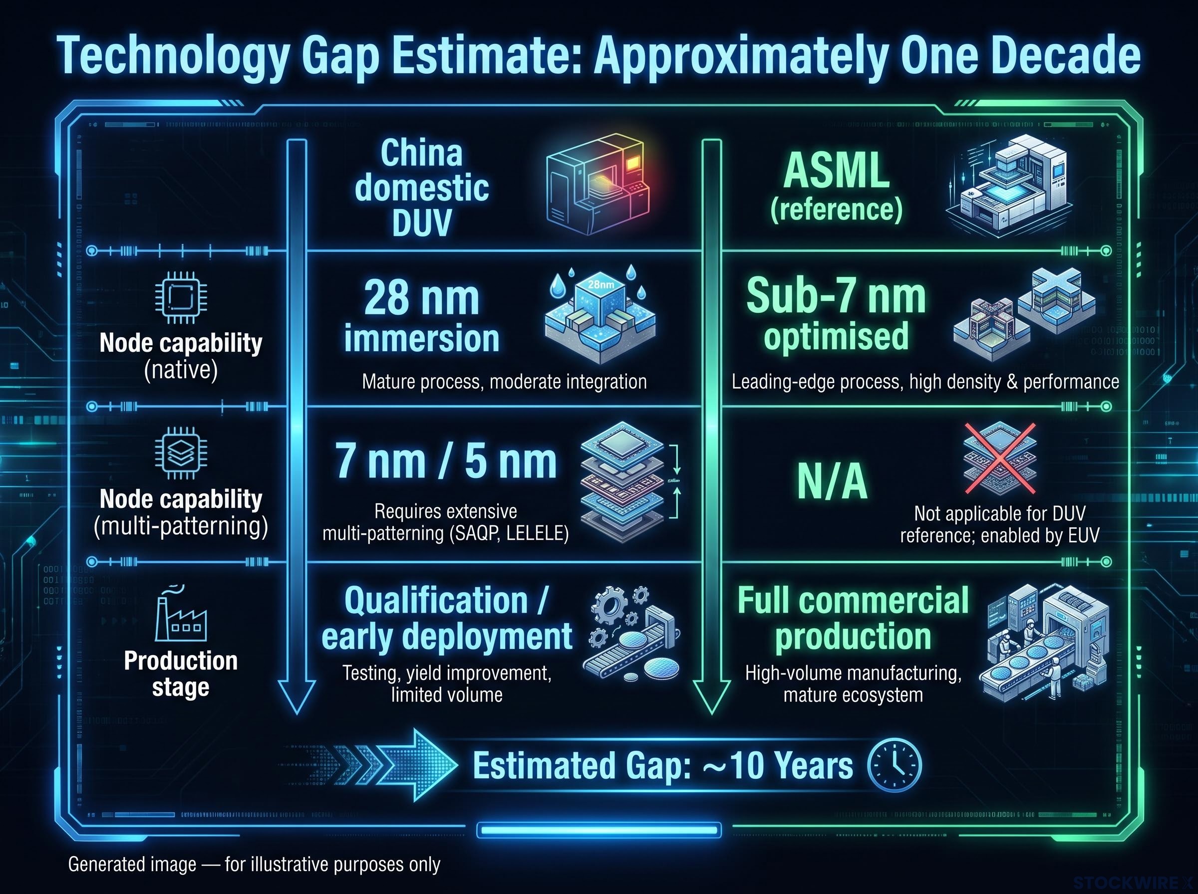
New DUV tools typically require at least one year of iterative tuning in fabs before reaching production-worthy stability and yields. China’s domestic EUV programme, the next-generation technology beyond DUV, remains at laboratory and prototype stage, years from commercial readiness.
| Metric | China domestic DUV | ASML (reference) |
|---|---|---|
| Units shipped / planned (2026) | ~5 immersion DUV tools | 131 immersion DUV + 48 EUV systems (2025 actuals) |
| Units planned (2027) | ~20 immersion DUV tools | Planned growth, particularly in EUV |
| Node capability (native) | ~28 nm immersion | Sub-7 nm optimised |
| Node capability (multi-patterning) | Potentially 7 nm / 5 nm (lower yield, higher cost) | N/A (EUV handles sub-7 nm directly) |
| Technology gap estimate | Approximately one decade behind leading ASML DUV | Benchmark |
| Metric | China domestic DUV | ASML (reference) |
|---|---|---|
| Subsystem localisation | Partial; some subsystems still imported | Fully integrated, global supply chain |
| Production stage | Qualification / early deployment | Full commercial production |
| Fab readiness timeline | At least 1 year of tuning required post-delivery | Established install base |
| EUV status | Laboratory / prototype stage | Commercial EUV fleet operational |
The scale and ecosystem gap tells you that ASML’s multi-year revenue runway from existing relationships with leading-edge fabs is not yet structurally threatened by this development, even if the long-term competitive trajectory is shifting.
High NA EUV adoption timelines at Intel, Samsung, and TSMC represent a separate revenue trajectory for ASML that sits entirely outside the China DUV competitive frame, with UBS projecting 37% year-over-year EUV revenue growth in 2027 as that inflection begins to materialise.
The BIS export control framework governs which lithography tools and components U.S. and allied suppliers can legally ship to Chinese fabs, making its licensing thresholds the regulatory ceiling against which any domestic Chinese capability milestone must be measured.
Why assembling the machine is only part of the problem
A lithography scanner is only as valuable as the surrounding process ecosystem. Precision optics partners, resist chemistry (the light-sensitive material that transfers circuit patterns onto wafers), metrology tools, and process know-how built through years of co-optimisation with fabs all form part of the moat. ASML and its allied suppliers have spent decades integrating these systems.
Partial import dependence for subsystems is a structural vulnerability for China’s programme, not just a near-term inconvenience. It means the domestic DUV supply chain remains exposed to future control escalation. A fully localised, maintainable, upgradeable tool is a categorically different achievement from a scanner that still relies on imported components for critical functions.
A five-step framework for reading any geopolitical tech headline
The China DUV story is today’s case. The next one will involve a different technology, a different country, or a different policy trigger. What stays constant is the process for evaluating it. Each step below answers the question the previous one leaves open, applied directly to the live DUV case.
1. Assess source and timing. Who is reporting, and what else is happening? The Information’s staff byline cited anonymous sources. The story landed while the MATCH Act was advancing through Congress between April and July 2026. Reports highlighting Chinese breakthroughs during active export-control negotiations can function as information signals within policy dynamics, not just neutral disclosures. Treat any single, anonymously sourced story at a politically sensitive moment as a hypothesis, not a confirmed fact, until corroborated.
2. Drill into the underlying numbers. If a headline says “mass production,” ask: how many units, to which customers, at what timeline? Here the answer is approximately five systems in 2026, roughly 20 in 2027, targeting 28 nm natively with multi-patterning to reach 7 nm, with overlay and stability gaps compared to ASML. The correct characterisation is early-stage ramp, not a fully formed competitive threat.
From numbers to risk classification and policy mapping
3. Separate milestone risk from capability risk. Milestone risk is evidence that the technical problem is tractable inside China: a working immersion DUV scanner, assembled with domestic participation, is a legitimate engineering achievement. Capability risk is something different entirely. It arises only when tools are deployed at scale (dozens to hundreds of units), yields and uptime match global norms, and the surrounding ecosystem supports competitive cost per transistor.
“Treat milestones as sentiment and volatility events. Treat capability at scale as thesis-changing events.”
The China DUV story sits firmly in milestone territory. That distinction determines whether you revise your thesis or simply log the development.
4. Map the policy dimension. Analytical work on the “lithography loophole” argues that China can leverage hundreds of existing DUV tools, plus upgrades and multi-patterning, to approach near-frontier logic dies even without new EUV imports. This suggests controlling the servicing and upgrading of older DUV tools may matter as much as blocking new sales. The outcome investors should weigh most carefully is a double loss: Western suppliers forfeit their China revenue while export controls nonetheless fail to arrest China’s technological advance. Map each report explicitly onto what the controls were designed to prevent (sub-14 nm at volume), whether the reported capability actually crosses that line, and how it interacts with specific companies’ China revenue exposure.
Export control risk channels for ASML extend beyond any single DUV headline, encompassing potential Bureau of Industry and Security investigations, tighter multilateral DUV controls, and government relationship friction that can each affect the multiple independently of fundamental earnings delivery.
5. Check scale, ecosystem, and follow-through signals. Even if the initial report is broadly correct, investment impact depends on what happens next. Are leading Chinese fabs moving from testing single units to ordering fleets? Is wafer output on domestic tools growing to meaningful percentages of fab capacity? Is the shift from partially imported subsystems to fully local, maintainable tools actually occurring? Update your thesis only as those observable metrics shift.
Running each new geopolitical tech claim through this sequence lets you distinguish whether a headline warrants a thesis review or simply a note in your monitoring log. That distinction is where informed investors find their edge over reactive ones.
What changes in the investment thesis, and what does not
The evidence presented across the preceding sections earns a specific verdict. Here is what the China DUV story changes, and what it leaves intact:
- What has incrementally shifted: The long-term case that China will build a domestic lithography stack is stronger. The technical problem is demonstrably tractable inside China, and the qualification-phase ramp provides tangible proof of engineering progress.
- What has not changed: ASML’s current multi-year revenue runway from existing fab relationships, the ecosystem moat from decades of optics, resist, metrology, and service integration, and the status of China’s EUV programme, which remains at prototype stage.
- What the selloff implied vs. what the data support: The 27 July 2026 selloff priced in a competitive displacement narrative. The underlying data describe a five-to-twenty-unit, qualification-phase ramp with tools approximately one to two nodes behind ASML’s leading immersion systems.
Headline risk today is high. Fundamental risk has risen incrementally but not discontinuously. There is more evidence of Chinese progress, but the gaps in scale, yield, ecosystem, and EUV remain substantial.
The gap between where the headline sent the stock and where the fundamentals actually sit is the definition of a mispricing opportunity. The investor who ran the five-step framework before reacting is the one positioned to evaluate it clearly. This is a signal to update long-term scenarios, not a trigger to exit semiconductor positions.
Building your watchlist for the next chapter of this story
The analytical framework produces a specific operational output: the metrics and events that would elevate China’s DUV progress from milestone risk to capability risk. Track these:
- Deployment counts: How many domestic DUV units are installed and operating at SMIC, Hua Hong, and CXMT beyond the initial pilot units.
- Node classes in production: Whether fabs are actually running 28 nm or sub-28 nm processes on domestic tools at meaningful volumes.
- Yield and defect disclosures: Any third-party or fab-level data on wafer yield rates from domestic DUV tools.
- Subsystem localisation progress: Movement from partially imported to fully domestic component stacks.
- Capex allocation: Whether leading Chinese fabs are committing material capital budgets to domestic tool procurement versus continued reliance on existing Western equipment.
- MATCH Act and related legislation: Final passage, scope, and enforcement mechanisms, and their impact on ASML and peers’ China revenue guidance.
- EUV prototype milestones: Any movement from laboratory to pilot or commercial stages for China’s domestic EUV programme.
- Export-control threshold crossings: Whether reported domestic capability approaches the sub-14 nm at volume threshold that controls were designed to prevent.
The EUV distinction matters: China’s domestic EUV programme remains at laboratory and prototype stage. That is categorically different from the DUV development stage, and conflating the two is a common analytical error. Movement toward pilot or commercial EUV would represent a higher-order signal than any DUV update.
Knowing which specific metrics to track means you will not need to rely on headlines to tell you when the story materially changes. You will see the shift in observable data before the next front-page report arrives.
The headline was the event; the fundamentals are the thesis
The 27 July 2026 selloff was a headline risk event, not a fundamental risk event. The evidence supports treating it as such: five qualification-phase tools, a decade behind ASML’s leading systems, with an ecosystem moat that remains firmly with Western suppliers.
Geopolitical tech headlines will continue to surface in semiconductors. The five-step framework, assess sourcing, drill into numbers, separate milestone from capability risk, map the policy dimension, and check for follow-through, gives you a repeatable process for each one. Investors with that process are structurally better positioned than those reacting to framing.
China’s domestic lithography progress is real and directionally significant. But the timeline from qualification-phase pilot to ASML-competitive industrial scale is measured in years, not quarters. That timeline is what the investment thesis should be anchored to.
For investors wanting to place the 27 July 2026 semiconductor selloff within a broader market context, our full explainer on the chip selloff classification framework examines BofA’s SOX underperformance indicators and the specific metrics that distinguish a recoverable trade-shock episode from a full cyclical downturn.
This article is for informational purposes only and should not be considered financial advice. Investors should conduct their own research and consult with financial professionals before making investment decisions. These statements are speculative and subject to change based on market developments and company performance.