Adisyn Cracks Graphene Deposition Below 450°C Targeting Chip Industry’s Copper Barrier
Adisyn demonstrates graphene deposition breakthrough targeting semiconductor industry’s copper bottleneck
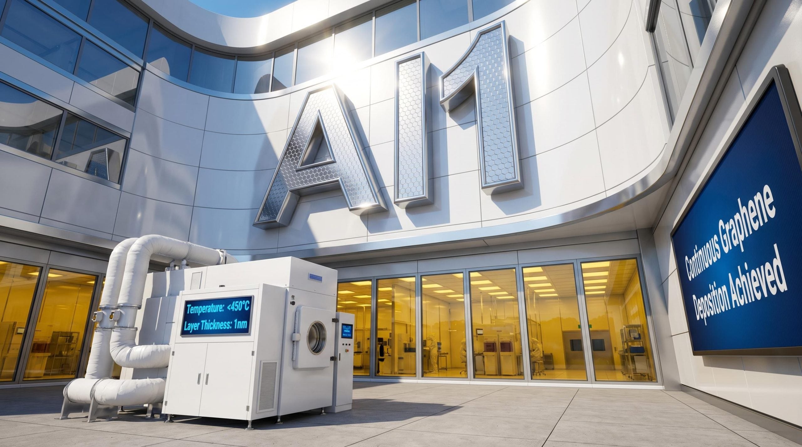
Adisyn Limited (ASX: AI1) has demonstrated continuous graphene layer deposition on a 1cm² coupon using an industrial Atomic Layer Deposition (ALD) system at temperatures well below the semiconductor industry’s thermal ceiling of approximately 450°C. The result addresses a widely recognised bottleneck in advanced chip manufacturing — the performance limitations of copper interconnects — and positions the company to enter industry collaboration discussions with Tier 1 semiconductor manufacturers.
The ~1nm graphene layer was deposited using Adisyn’s patented ALD methodology and proprietary precursor chemistry, developed through wholly-owned subsidiary 2D Generation. With over 1 trillion chips produced annually across the global semiconductor industry, Adisyn is targeting high-performance segments including AI accelerators, GPUs, CPUs, advanced mobile processors, and networking chips where interconnect performance directly constrains device capability.
When big ASX news breaks, our subscribers know first
Why copper interconnects are holding back advanced chips
Interconnects are the microscopic wiring that connects billions of transistors inside semiconductor chips. As chip geometries shrink to sub-2nm nodes, copper interconnects suffer from increasing electrical resistance, heat generation, and power loss. These constraints limit chip performance, energy efficiency, and further miniaturisation — a critical barrier as the industry pushes toward the next generation of AI and high-performance computing devices.
Graphene has been recognised for decades as a potential solution due to its superior electrical conductivity and thermal properties. However, adoption has stalled because no manufacturing process has previously achieved graphene deposition within the constraints of existing semiconductor fabrication facilities — specifically using standard equipment and temperature limits compatible with commercial production.
Copper’s limitations versus graphene’s advantages:
- Copper: Increasing resistance at nanoscale dimensions, significant heat generation, power loss at advanced nodes
- Graphene: Superior electrical conductivity, exceptional thermal properties, maintains performance at nanoscale dimensions
- Manufacturing barrier: Graphene growth historically required temperatures or processes incompatible with semiconductor fabrication
This breakthrough targets the intersection of AI infrastructure buildout and semiconductor scaling constraints, positioning Adisyn at a critical juncture in the industry’s evolution.
What makes this result different from laboratory demonstrations
Semiconductor fabrication facilities do not adopt materials requiring entirely new manufacturing approaches. The industry operates within tightly controlled parameters — thermal budgets, equipment standards, and process compatibility — that exclude technologies developed in laboratory environments using non-standard methods.
Adisyn’s result demonstrates the convergence of three requirements the semiconductor industry has struggled to achieve simultaneously:
- Use of industrial ALD system — not lab-scale equipment or transfer-based graphene methods
- Operation within semiconductor-compatible temperatures — below the ~450°C thermal ceiling required by fabrication facilities
- Continuous graphene layer formation — confirmed via Transmission Electron Microscopy (TEM) and Raman Spectroscopy characterisation tests
Kevin Crofton, Chairman
“This is an important step – not just for Adisyn, but in the context of what the semiconductor industry has been trying to achieve. Producing graphene on an industrial ALD system, rather than a lab environment and at low temperature, is what starts to make this relevant from a manufacturing perspective.”
Industrial compatibility removes a historical barrier that has kept graphene theoretical rather than manufacturable. The process is based on Adisyn’s patented ALD methodology and proprietary precursor chemistry developed specifically to enable graphene growth within semiconductor manufacturing constraints.
Temperature compliance opens fabrication facility doors
Any new material must integrate within existing thermal budgets to be considered for semiconductor manufacturing. Historically, graphene growth required significantly higher temperatures than the ~450°C ceiling imposed by fabrication facilities, excluding it from commercial consideration regardless of material performance.
This result positions Adisyn’s process within the operating window semiconductor fabs require. The deposition process operates well below the industry’s thermal limit, a key barrier that has historically prevented graphene adoption in interconnect applications.
Kevin Crofton, Chairman
“Temperature has always been one of the major hurdles. If you’re outside the thermal limits of a fab, you’re not even part of the discussion. What we’ve demonstrated here is that we are operating inside that window.”
Technical validation confirms continuous graphene layer
Characterisation testing used Transmission Electron Microscopy (TEM) and Raman Spectroscopy to confirm continuous graphene layer formation across the 1cm x 1cm coupon. Continuous layer formation is a prerequisite for any material being considered for interconnect applications — the graphene must be uniform with no discontinuities to ensure electrical performance and reliability in semiconductor devices.
| Parameter | Result | Industry Requirement | Status |
|---|---|---|---|
| Deposition Method | Industrial ALD | Standard fab equipment | Achieved |
| Temperature | Below 450°C | <450°C thermal ceiling | Achieved |
| Layer Coverage | Continuous | No discontinuities | Confirmed |
| Layer Thickness | ~1nm | Nanoscale precision | Achieved |
The TEM analysis revealed a ~1nm graphene layer on the copper substrate, with the layer thickness measured at d=3.4±0.3Å. Raman Spectroscopy characterisation confirmed the presence of graphene through spectral signature analysis, validating the material composition and structural integrity.
Kevin Crofton, Chairman
“What we’ve demonstrated here is continuous graphene across the copper surface – and that’s fundamental. It is the first step in delivering an interconnect solution to the semiconductor industry.”
The next major ASX story will hit our subscribers first
Next steps and pathway to commercialisation
The company will now advance the programme through three phases targeting industry-quality film production and scale-up:
- Recipe optimisation to improve film quality and material performance
- Repeatability trials to confirm the process can be consistently reproduced
- Scale-up from coupon-level (1cm²) to wafer-level substrates
The next key milestone will be demonstrating repeatable industry-quality films, followed by wafer-scale validation and engagement with industry partners. Adisyn will commence engagement with semiconductor industry participants to explore collaboration, validation, and integration pathways.
Kevin Crofton, Chairman
“Now it’s about doing it again and again – consistently, with high quality – and then scaling it. That’s the phase that ultimately determines whether this becomes a commercial process.”
The commercial opportunity ahead
By the early 2030s, billions of advanced computing chips will be produced annually to support demands from AI infrastructure, high-performance computing, and next-generation mobile devices. The global semiconductor industry already produces over 1 trillion chips annually, with Adisyn targeting the high-performance segments where interconnect performance directly constrains device capability.
Once repeatable high-quality film properties are achieved at scale, this technology has the potential to enable graphene to replace copper in next-generation semiconductor interconnects, unlocking the next generation of advanced chip manufacturing.
Kevin Crofton, Chairman
“The industry has known for a long time that graphene could address interconnect challenges. The difficulty has always been how to get there in a way that fits within existing manufacturing environments. This starts to show that there is a scalable pathway to adopt graphene as an interconnect material.”
The company’s Tier 1 engagement strategy will focus on collaboration with global semiconductor manufacturers to validate the technology within commercial fabrication environments and establish integration pathways for production deployment.
Want the Next Semiconductor Breakthrough in Your Inbox?
Join 20,000+ investors receiving FREE breaking ASX Tech news delivered within minutes of release, complete with in-depth analysis. Click the “Free Alerts” button at Big News Blast to get market-moving announcements the moment they break, with expert coverage already done for you.